
QUEST, A TCI-Based 3D-Stacked SRAM Neural Processor
![]() In the last few years, advancement in packaging has created a boon for heterogeneous integration solutions. Although the industry is trying to solve a plethora of problems, perhaps none are as significant as the memory bandwidth. Many of the current solutions that are either on the market (e.g., HBM) or being researched involve the use of through-silicon vias (TSVs). While TSVs have been the go-to method for enabling the stacking of memory directly on top of logic, they are not the only solution. One alternative technology is ThruChip Interface (TCI), a near-field inductive coupling die-to-die wireless communication technology. For the time being, TCI still falls in the research category albeit at least one company is currently pursuing this technology in a commercial product.
In the last few years, advancement in packaging has created a boon for heterogeneous integration solutions. Although the industry is trying to solve a plethora of problems, perhaps none are as significant as the memory bandwidth. Many of the current solutions that are either on the market (e.g., HBM) or being researched involve the use of through-silicon vias (TSVs). While TSVs have been the go-to method for enabling the stacking of memory directly on top of logic, they are not the only solution. One alternative technology is ThruChip Interface (TCI), a near-field inductive coupling die-to-die wireless communication technology. For the time being, TCI still falls in the research category albeit at least one company is currently pursuing this technology in a commercial product.
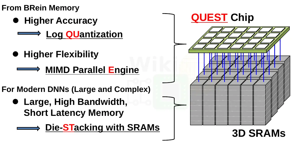
At this year’s ISSCC, the QUEST neural processor was presented. QUEST is an inference engine that uses stacked SRAM and TCI to incorporate a large amount of SRAM cache and sufficiently high bandwidth to sustain peak performance. The chip itself is a joint collaboration between Hokkaido University and Keio University. It’s worth noting that Keio University is also the original developer of TCI.
3D Stacking & System Architecture
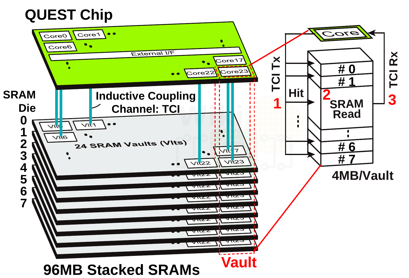
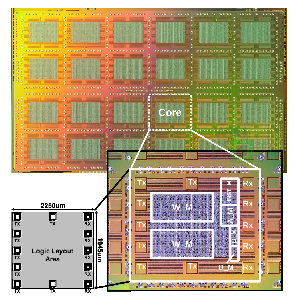
QUEST is a single 3D module comprised of 9 dies – 8 SRAM and a single logic die. Fabricated on TSMC’s CMOS 40nm Low Power process, all the dies are 121.55 mm² (14.3mm × 8.5mm). The actual QUEST logic chip, which incorporates 24 cores, sits on top of the SRAM stack for thermal reasons. The chip is logically partitioned into 24 vaults. Each vault includes a single core and 4 MiB of SRAM which is made of 512 KiB chunks from each of the SRAM dies directly below it. Parallel channels were implemented across the chip to facilitate multiple independent stacked SRAM accesses.
For communication, QUEST uses ThruChip Interface (TCI) which requires no special modifications to a base CMOS process. Furthermore, TCI can permeate metal layers and active devices (being magnetic fields) which means the coils can be placed on top layers. For power, QUEST uses TSVs. However since there are multiple parallel connections, problems such as open-contact failures can largely be eliminated. It’s worth noting that ideally, TCI is intended to go along with highly-doped silicon vias (HDSVs) which is a “wire-less” (but not wireless) power transmission technique. HDSV uses deep impurity wells to conduct electricity across chips instead of actual TSVs or wires, however, the technology is in early research and as far as we know has not been demonstrated in any actual TCI prototype chips (it also relies on fairly recent advancements in wafer thinning techniques).
The QUEST logic die incorporates 24 cores. Each of the 24 cores operates at 300 MHz while the individual TCI channels run at 3.6 GHz. There is a single channel per core which consists of 7 transmission coils and 5 receiver coils. The read/write latency is always 3 cycles. This includes the TCI trip time and is uniform over all eight of the stacked SRAM dies. This works out to 9.6 Gb/s per vault or 28.8 GB/s per module.
Logic
The die incorporates 24 MIMD parallel cores. Each core is linked in a mesh topology to its four neighbors – north, south, east, and west – as well as a tree-structured global network. Additionally, every core is linked to its corresponding vault SRAM via the TCI interface. Direct memory accesses are done by the dedicated DMAC unit which handles both vault SRAM memory accesses as well as the 7.68 MiB of on-die shared memory (intra-core).
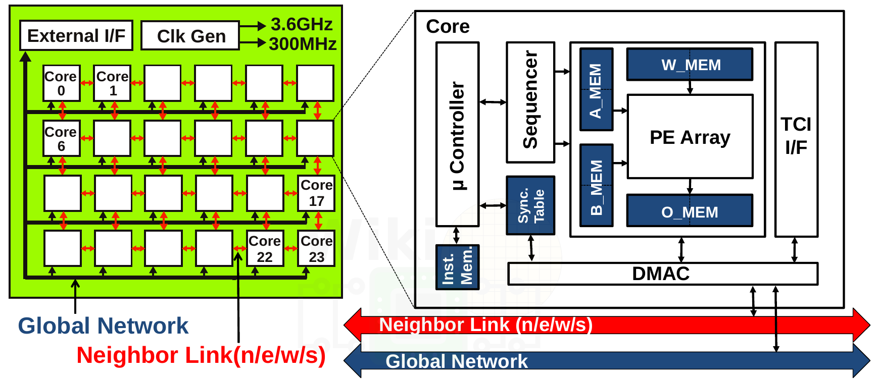
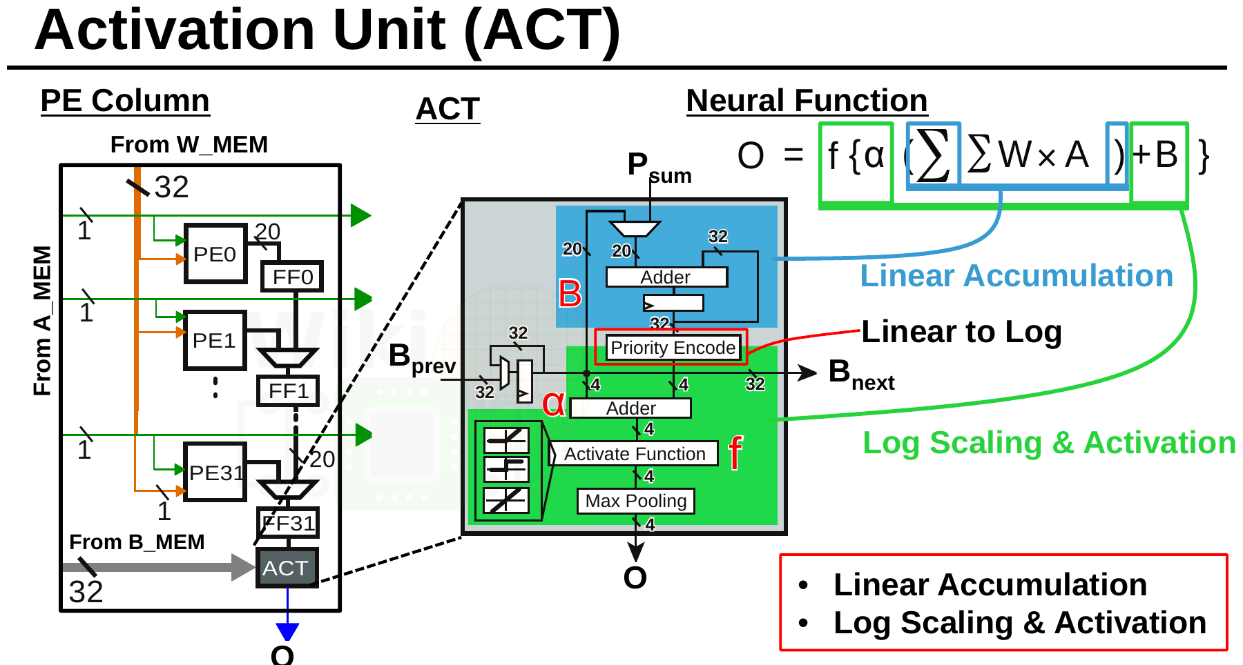
QUEST uses a relatively simple bit-serial architecture. The bit-serial PE array consists of 16 columns and 32 rows. Double-buffered weights (stored in W_MEM) are distributed in parallel while double-buffered activations (stored in A_MEM) are broadcasted in parallel to all the rows. Each PE generates a partial dot product in parallel. The results are shifted and accumulated at the ACT unit.
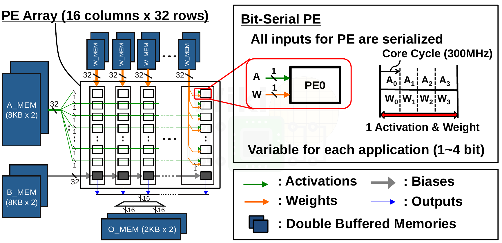
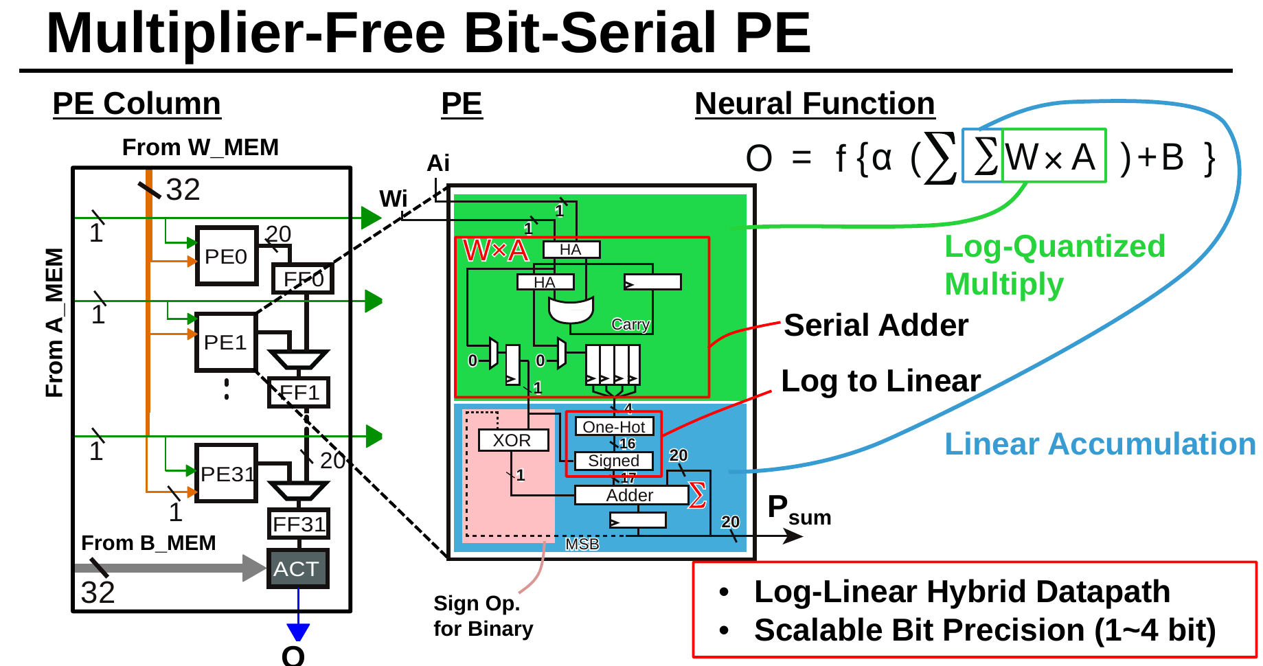
Bias stored in B_MEMs are shifted into the ACT unit located at the end of each column. The ACT unit applies biases, scaling, and the activation function and then writes the output into the out memory (O_MEM).
Mapping Networks
For a CNN such as AlexNet, processing can be done all 24 cores, layer by layer, with input and output results intermediately being stored in the SRAM. For the CONV layers clever placement of ‘virtual core clusters’ can be done in order to form clusters where the output channel is mapped (taking advantage of the physical locations of the cores on the mesh). For the fully connected layers, an even mapping of the output neurons is applied to all the cores. In this network, activations from one core’s SRAM vault will inevitably have to be read by another core. Those operations will be done through the on-die networks and through the TCI interfaces.
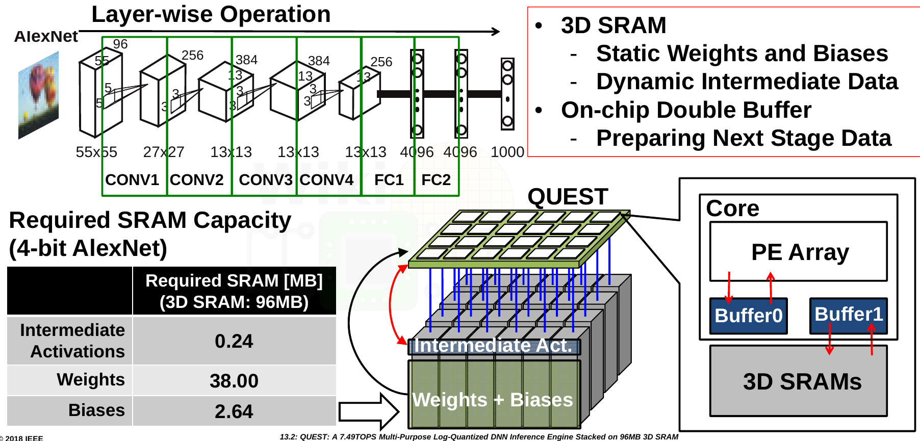
Supporting precision of 1 to 4 bits, QUEST dissipates 3.3 W (includes the stacked SRAM) at a nominal voltage of 1.1 volts and can achieve a peak performance of 1.96 TOPS for 4b and 7.49 TOPS for 1b. For AlexNet at 4b, the effective performance is 1.825 TOPS (76.7% Top-5 Accuracy).
–
Spotted an error? Help us fix it! Simply select the problematic text and press Ctrl+Enter to notify us.
–