
VLSI 2018: GlobalFoundries 12nm Leading-Performance, 12LP
 Though not dead, Moore’s Law is certainly getting expensive. In the wake of the sharply increasing costs of developing new leading-edge nodes, foundries are putting more effort into extending the life of existing nodes through modest performance and area improvements. At the 2018 Symposia on VLSI Technology and Circuits, GlobalFoundries opened up about their 12nm nodelet, an enhanced extension of their 14nm process. The improved process was presented by Hsien-Ching Lo, technology development deputy director at GlobalFoundries.
Overview
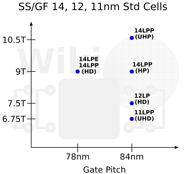
Previously we discussed Samsung’s 11LPP process which was also presented at the VLSI conference. Both Samsung’s 11LPP and GlobalFoundries 12LP have their roots in Samsung’s original 14nm process, a process GlobalFoundries later licensed and has been using in their mass production lines since 2016. Samsung introduced a number of standard cells for their 14nm process: their original 9T 14LPE standard cell (the same as 14LPP HD cell) and two high-performance cells – 9T (HP) and 10.5T (UHP).
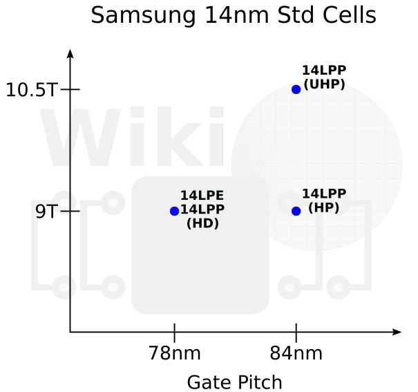
Note that the two high-performance cells use a relaxed poly pitch of 84nm whereas the high-density cell uses the original 78nm gate pitch. For their own 11LPP node, Samsung introduced a new 6.75T high-density cell based on the relaxed gate pitch.
Reference Technology
Throughout this article, we report on various area and performance improvements versus a 14nm node. Those comparisons are done against Samsung-GF 14LPP process, not 14LPE. This is slightly different from the reference technology that was used for 7LP which we reported about from IEDM which uses Samsung’s original 14nm process as the reference technology.
12nm Leading Performance (12LP)
GlobalFoundries 12LP (12nm Leading-Performance) is a full platform extension of their 14LPP process. What this means is that for the most part, GlobalFoundries 14nm platform is compatible with 12LP. GlobalFoundries has also widened their platform offering to a number of other key sectors including the automotive industry with automotive grade 2 compliant fabs and a wider portfolio of RF IPs.
In order to introduce improvements while minimizing design rework, GlobalFoundries kept the design rules pretty much the same.
| GlobalFoundries 12nm vs 14nm | |||
|---|---|---|---|
| 14LPP (HP) | 12LP (HP, HD) | Δ | |
| Fin Pitch | 48 nm | 48 nm | 1.0x |
| Poly Pitch | 84 nm | 84 nm | 1.0x |
| Metal 2 | 64 nm | 64 nm | 1.0x |
This is in a slight contrast to both Samsung and TSMC which actually shrunk the BEOL. Lo explained that the choice to not touch the BEOL was done in order to maximize customers ease of migration from 14nm to 12nm. It’s worth pointing out that Samsung actually uses their 10nm process BEOL which has been in high-volume status for sometimes now, something that GlobalFoundries cannot do.
New HD Cell
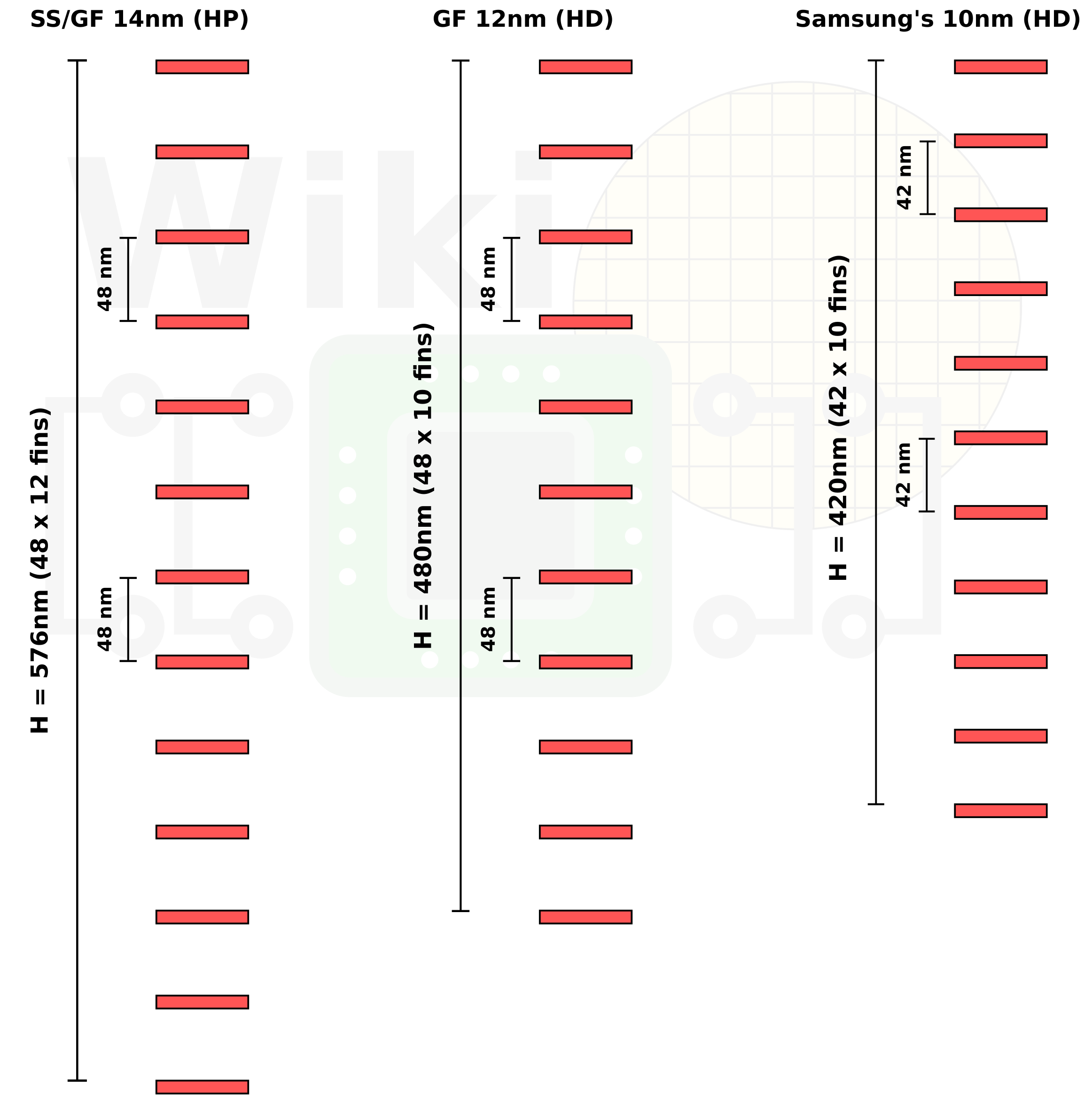
For 12LP, GlobalFoundries introduced a new 7.5T library.
| GlobalFoundries 12nm vs 14nm | |||
|---|---|---|---|
| 14LPP (HP) | 12LP (HD) | ||
| Tracks | 9T | 7.5T | |
| Cell Height | 576 nm | 480 nm | |
| Metal 2 | 64 nm | 64 nm | |
The new high-density cell is very short, getting closer in height to Samsung’s 10nm.
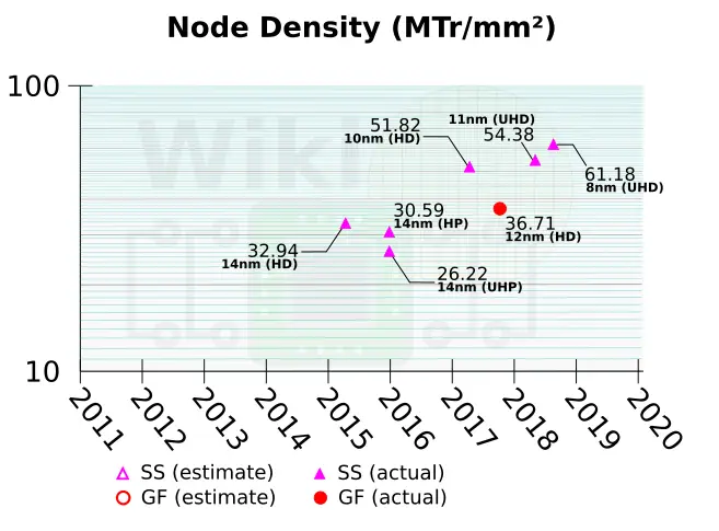
Plugging in GlobalFoundries 12LP high-density (HD) cell using Intel’s density metric gives us 36.71 MTr/mm², roughly 1.2x improvement over the 9T 14LPP cell. GF reported a more modest 12% logic area scaling number.
–
Spotted an error? Help us fix it! Simply select the problematic text and press Ctrl+Enter to notify us.
–