
TSMC Ramps 5nm, Discloses 3nm to Pack Over a Quarter-Billion Transistors Per Square Millimeter
Results were mixed from TSMC first quarter 2020 financial results. Amid pandemic, the company saw net revenue of $10.31 billion, a decrease of just under one percent over its fourth-quarter revenue. TSMC says the drop is less than seasonality due to stronger HPC-related demand and 5G smartphone ramp.
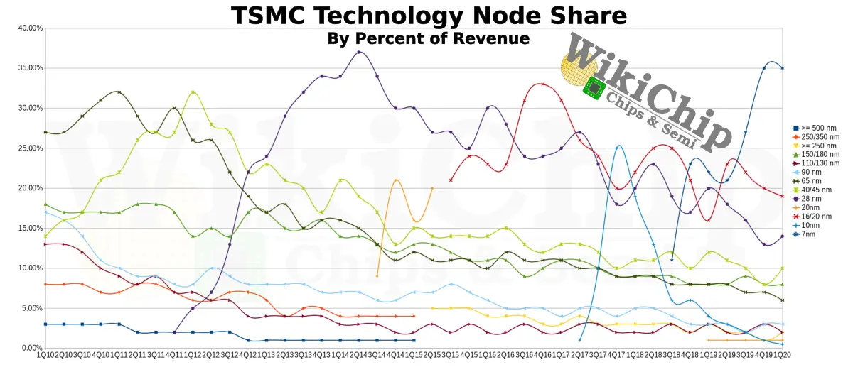
In the first quarter of 2020, the company’s flagship 7-nanometer N7 node contributed 35% of wafer revenue. This is the same amount as the previous quarter, suggesting TSMC N7 has reached its apex. TSMC saw a sharp drop of 9%, quarter-over-quarter, in smartphone revenue to account for 49% of revenue. This was partially offset by an increase of 3% from the HPC market which now makes up 30% of revenue. Desktop consumer electronics (DCE) were up a whopping 44% in Q1 to account for 5% of total revenue. Interestingly, both 16-nanometer and 10-nanometer revenue share dropped by 1% and 0.5% respectively over the previous quarter. This corresponds with a weaker demand for yesteryear SocS without renewed demand for newer SoCs. As a consequence, both 45 nm and 65 nm nodes made up around one percent high in terms of wafer revenue. N16 and below (which TSMC bundles together as advanced technologies) account for 55% of total wafer revenue.
Further Reading:
- TSMC 7nm HD and HP Cells, 2nd Gen 7nm, And The Snapdragon 855 DTCO
- TSMC Talks 7nm, 5nm, Yield, And Next-Gen 5G And HPC Packaging
- TSMC Q4: 7nm Dominates Revenue, Preps 5nm Ramp, 6nm By EOY
- 7nm Boosted Zen 2 Capabilities but Doubled the Challenges
TSMC expects its second-quarter revenue to remain flat – between $10.1 and $10.4 billion. The company expects smartphone sales to remain weak throughout the second quarter. C.C. Wei went on to say that “while we have not seen significant order reduction from our customers so far, we do observe supply chain dislocation and weaker market demand from COVID-19 in the first half of this year”. “We now forecast the overall semiconductor market, excluding memory growth, to be flat to slightly decline. While foundry industry growth is suspected to be high single-digit to low teens digit. For TSMC, although uncertainty exists, we believe we can do better at mid- to high teens percentage in 2020 in US Dollar terms” he added. All TSMC statements are based on the assumption that COVID-19 stabilizes by June.
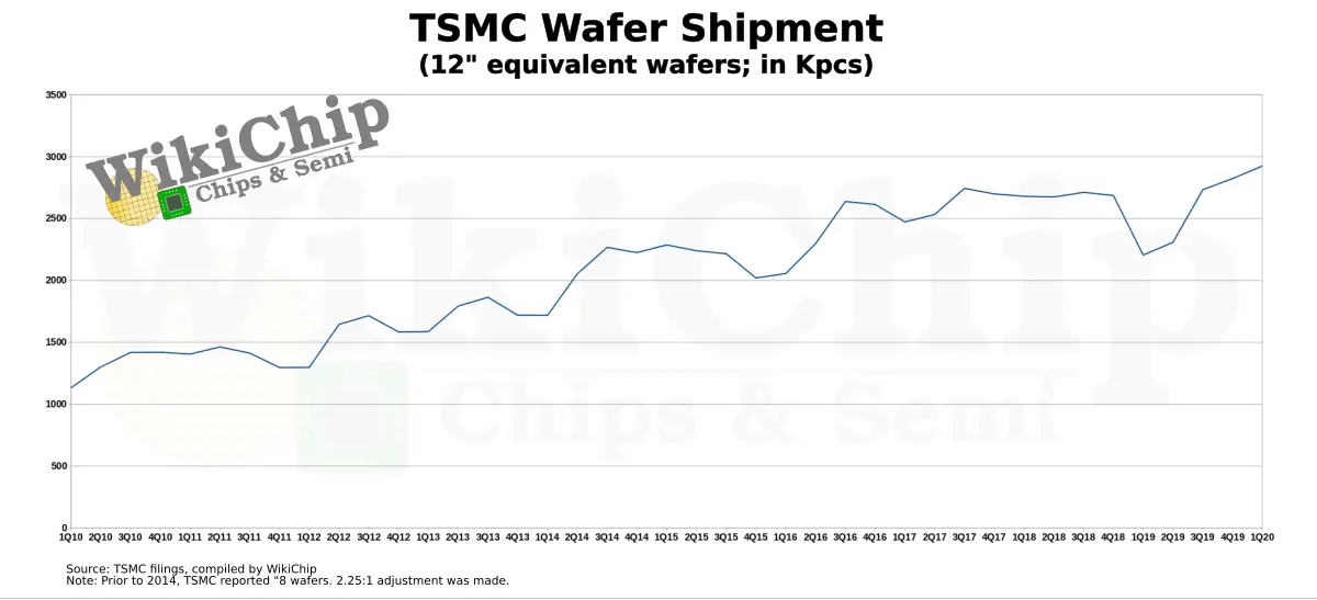
Despite the shaky quarter, the company shipped a hair under 3 million wafers – the highest volume ever reported for the second quarter in a row.
COVID-19
TSMC suspended non-critical business travel since January and has implemented mandatory screening for all visitors. The company reported no disruption to operations due to COVID-19. On March 18th a single employee tested positive. This employee has since recovered. All other employees that were in contact with that individual underwent mandatory quarantine, have since tested negative, and have returned to work. Since March and wherever possible, TSMC has switched to working from home.
Ramp-up Status
- N7 is in its 3rd year of ramp
- N7+ entering its 2nd year of ramp using EUV
Last year TSMC announced a new N6 node. The company says this node builds on the EUV learning from its N7+ node but maintains a clear migration path for N7 customers. To that end, N6 features design rules fully-compatible with N7. N6 features a single EUV layer more than N7+. N6 has already entered risk production and is on track for volume production before the end of this year.
CapEx
Despite COVID-19, TSMC affirms a 2020 capital expenditure budget between $15 and $16 billion.
N5 Status
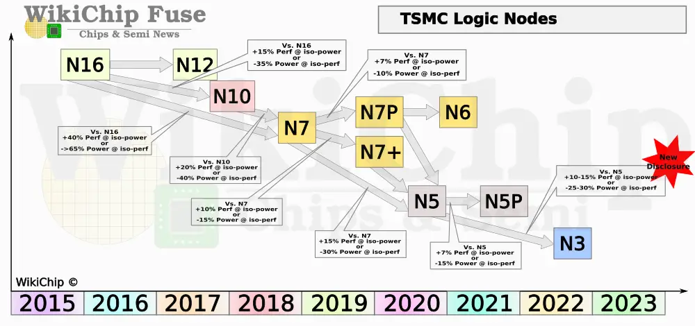
TSMC’s 5-nanometer node entered risk production early last year. C.C. Wei confirmed that N5 is now in volume production with good yield. We have recently covered TSMC 5-nanometer node disclose from a number of conferences. The node will deliver around 1.8x improvement in density along with 15% higher speed at iso-power or, alternatively, 30% lower power at the same speed. N5, like N7, is expected to remain a long-lasting node. “We expect a very fast and smooth ramp of N5 in the second half of this year driven by both mobile and HPC applications,” C.C. Wei added. TSMC estimates that N5 will contribute about 10% of wafer revenue in 2020. TSMC is observing a higher number of tape-outs compared to N7 at the same period of time during their ramp.
Further Reading:
N3
This earnings call marks the first time TSMC started disclosing actual information about its 3-nanometer (N3) node. C.C. Wei says the company’s N3 remains on track with risk production scheduled for 2021. TSMC is targeting volume production in the second half of 2022. The company says that after evaluating all the possible device technology options, it had decided to continue with FinFET for N3 due to its maturity, performance, and cost advantages.
In terms of density, TSMC says N3 will be another full node stride over N5 with a density improvement of 1.7x over N5. Going based on Wei’s word, our initial estimates for the N3 is that it will offer a cell-level density of just under 300 million transistors per millimeter square. Once we’re able to fully confirm the N5 node density, a more accurate density prediction of the N3 node will be possible.
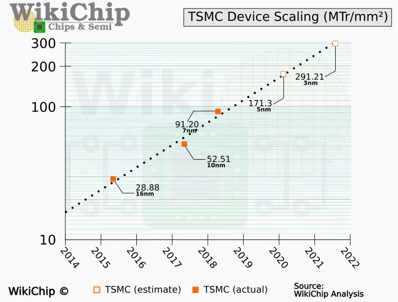
In terms of performance and speed, compared to N5, TSMC says N3 will provide 10-15% speed improvement at iso-power or 25-30% power reduction at iso-speed.
–
Spotted an error? Help us fix it! Simply select the problematic text and press Ctrl+Enter to notify us.
–