
IEDM 2018: Intel’s 10nm Standard Cell Library and Power Delivery
![]() The standard cell library contains an assortment of primitive cells that implement common logic functions. Cells include simple gates such as AND and OR but also more complex components such as multiplexers, buffers, latches, and flip-flops. Those cells underpin the entire microprocessor design. It defines what’s possible, how big, how fast, and at what power and frequency ranges. Often times the construction of the cells remain a secret behind a wall of NDAs. At the 64th IEEE International Electron Devices Meeting (IEDM) that was held in San Francisco in December, we got a rare look into the construction of such library – specifically, that of Intel’s 10-nanometer standard cell. The excellent presentation was delivered by Dr. Xinning Wang, Engineering Manager at Intel’s Advanced Design Library Group.
The standard cell library contains an assortment of primitive cells that implement common logic functions. Cells include simple gates such as AND and OR but also more complex components such as multiplexers, buffers, latches, and flip-flops. Those cells underpin the entire microprocessor design. It defines what’s possible, how big, how fast, and at what power and frequency ranges. Often times the construction of the cells remain a secret behind a wall of NDAs. At the 64th IEEE International Electron Devices Meeting (IEDM) that was held in San Francisco in December, we got a rare look into the construction of such library – specifically, that of Intel’s 10-nanometer standard cell. The excellent presentation was delivered by Dr. Xinning Wang, Engineering Manager at Intel’s Advanced Design Library Group.
Std Cell
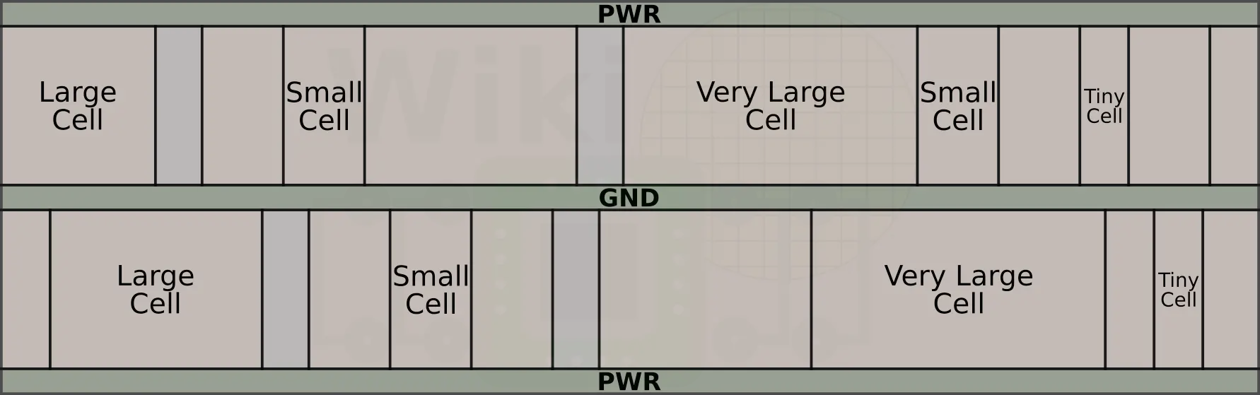
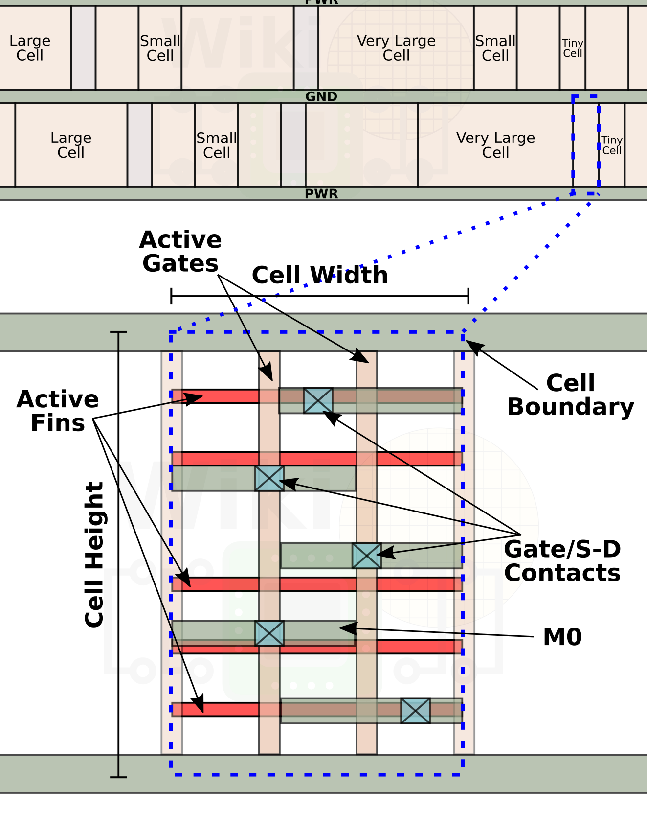
Standard cells are fixed-height blocks with variable width. Those cells have a predefined location for the power rails such that they can be easily linked together with other cells in the library. This helps simplify place and route but also various other analysis. Typically, this is done with the power rails running along the top of the cell while the ground rails run along the bottom. At the back end of the cells, you find a hierarchy of metal layers that are used for routing and interconnecting. The goal of the cells is to be more or less independent and modular such that they can be combined with other cells to form more complex logic. This is very much analogous to Lego pieces. Multiple standard cells are combined side by side to form defined rows of uniform height. This is done for well and diffusion mask continuity. In other words, this is done to allow deponent regions to span the entire length of the row. Within a row, many different types of cells can be placed – of varying widths. The width depends on the type of logic implemented. The narrower cells are referred to as being “smaller” while complex logic that results in very wide cells are referred to as “large cells”. In addition to logic cells, there are sometimes other types of cells such as filler cells (e.g., caps/decaps) and end caps which are used for voltage stability, isolation, and other similar applications (those are colored gray in our simplified diagram below).
Within each cell are the basic transistors. Below is an example of a FinFET CMOS cell. It has five active fins and two active gates. From that diagram, it can be seen how the number of poly gates can affect the cell width while the number of fins can affect the cell height.
Variants
The standard cell definitions for Intel’s 10-nanometer are very important since they serve as the foundational building blocks for most of their designs. As such, they were designed to work seamlessly with the industry standard auto-place and route (APR) physical design tools. Intel expects a very diverse portfolio of products for their 10-nanometer as a result of many of their recent acquisitions that will be migrated in-house from TSMC. On top of this, Intel is also looking to enter a number of new markets including the discrete graphics market. For their 10 nm, Intel’s strategy has been to offer enough standard cell options to provide designers with a sufficient degree of power-performance-area tradeoffs to deliver the best product for their needs. It’s worth noting that both reliability and design for manufacturability were taken into consideration at the very beginning of library definitions.
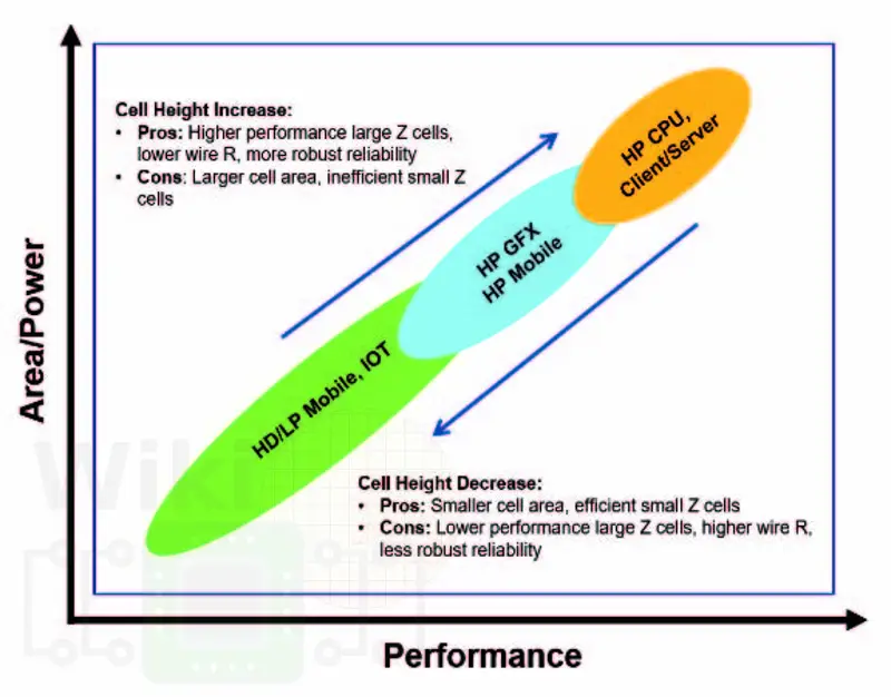
For their 10-nanometer, at the one extreme, Intel standard cells span all the way to IoT and low-power mobile applications which have relatively lower performance but are more optimized for power and density. On the other end of the spectrum are Intel’s ultra-high performance CPU designs which sacrifice power/area for very high performance. Those 10nm cells target frequencies greater than 5 GHz under 100% usage conditions. In between the two are high-performance mobile as well as high-performance graphics products which require a more balanced PPA.
The Rules of the Game
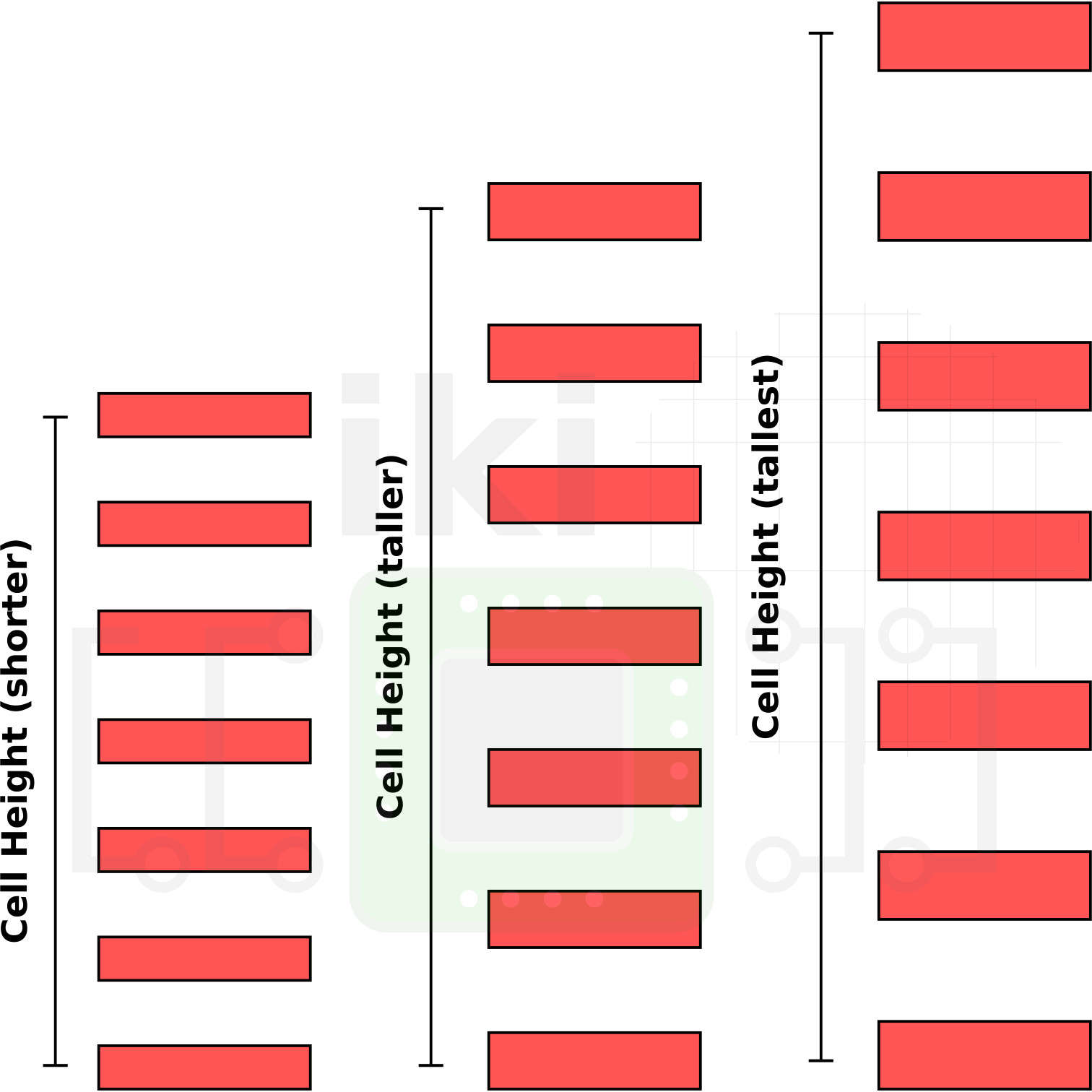
Intel’s 10 nm transistor design rules include a 34-nanometer fin pitch and a 54-nanometer gate pitch. Additionally, Intel introduced a single dummy gate (SDB) and contact over active gate (COAG). The SDB and COAG play a significant role in the design of the standard cell itself as we will show later. When the rest of the ground rules are fixed, the main power-performance-area (PPA) tradeoff modulator is the cell height. A shorter cell means higher density as more cells can be packed into the same silicon area. Likewise, taller cells incur area penalty, however, they provide the opportunity for accommodating more fins per transistor. Therefore controlling the cell height manipulates performance and area in a contradictory way.

When deciding on the cell height, another big consideration is the number of metal tracks that can be accommodated for efficient inter-cell connections. As with the case of the transistor fins, taller cells can accommodate more metal tracks. Interestingly, in Intel’s case, they are not actually taking advantage of that. Instead, they are keeping the metal tracks the same. What this allows them to do is to increase the wire width without sacrificing the track count. Wider wires also mean bigger vias – both result in significant reliability improvement against electromigration. As with everything else, this too is a compromise. For taller cells with wider wires, it means you end up with less efficient small cells. Likewise, with shorter cells with narrower wires, you end up with less efficient big cells.
The final consideration factor for the cell height is the power delivery scheme. This includes the power rails positions. These decisions have a lot of effect on the robustness and electromigration. The positioning is also important for i/o minimization.
–
Spotted an error? Help us fix it! Simply select the problematic text and press Ctrl+Enter to notify us.
–