
Inside Tesla’s Neural Processor In The FSD Chip
Among the many excellent presentations at the annual IEEE Hot Chips conference was Tesla’s FSD chip. Tesla first disclosed their Full Self-Driving (FSD) Chip in April at the company’s Autonomy Day. At the recent Hot Chips 31 conference Tesla provided some additional insight into some of the key components of the chip.
Tesla engineers had a number of major goals for the FSD chip and platform. They wanted to pack as many TOPS as possible within their power envelop. A main design point for the chip was high utilization of the chip at a batch size of one for safety reasons. It’s worth noting that FSD chip comes with a set of CPUs for general-purpose processing and a light-weight GPU for post-processing which are beyond the scope of this article. Those components have been detailed on our main WikiChip article.
Neural Processors
While most of the logic on the chip makes use of industry-proven IP blocks in order to reduce risk and accelerate the development cycle, the neural network accelerators on the Tesla FSD chip are a fully custom design made by the Tesla hardware team. They are also the largest component on the chip and is the most important piece of logic.
One interesting tidbit Tesla talked about is simulation. During development, Tesla wanted to validate their NPU performance by running its own in-house neural networks. Because they did not have emulation ready early on, they resorted to using the open-source Verilator simulator which they say managed to run 50 times faster than commercial simulators. “We used Verilator extensively to prove our design is very good,†said Venkataramanan, Sr Director Autopilot Hardware at Tesla.
There are two identical NPUs inside each FSD Chip – physically integrated one next to the other. When asked for the reason for having two instances of the NPU as opposed to something like a bigger unit, Tesla noted that the size of each individual NPU is a sweet spot for physical design (timing, area, routing).
ISA
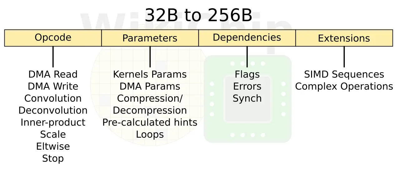
The NPU is an in-order machine with an out-of-order memory subsystem. The overall design is kind of a fancy state machine. The ISA consists of instructions with up to 4 slots with complex values. There are only eight instructions in total – two DMA read and write, three dot-product operations, and scaling and element-wise addition. The NPU simply runs through those commands until hitting the stop command which halts it. There is an additional parameters slot which can change the attribute of the instruction (e.g., different variations of the convolutional operation). There is a flags slot which is used for data dependencies handling. And there is another slot for extensions. This slot stores the entire micro-program sequence of commands which go to the SIMD unit whenever there is some complex post-processing. Because of this, instructions vary from 32 bytes all the way to very long 256 bytes. The SIMD unit is discussed in more detail later on.
Initial Operations
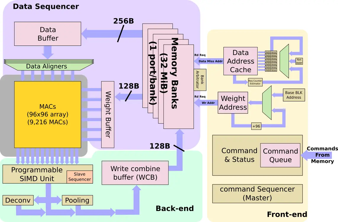
Programs for the NPU are initially resident in memory. They are brought into the NPU where they are stored in the command queue. The NPU itself is a very fancy state machine intended to considerably reduce the overhead of control. Commands from the command queue are decoded into the primitive operations along with a set of addresses for where the data needs to be fetched from – this includes for both the weights and the data. For example, if the sensor is a newly taken image sensor photo, the input buffers address will point to there. Everything is stored in a very large cache inside the NPU. There is no DRAM interaction from that onwards.
The cache is 32 MiB in capacity and is a highly banked with a single port per bank. Tesla noted that there is a sophisticated bank arbitrator that, along with some compiler hints, is used to reduce bank conflicts. Each cycle, up to 256 bytes of data can be read into the data buffer and up to 128 bytes of weights can be read into the weights buffer. Depending on the stride, the NPU may bring more than one line into the data buffer before operations begin in order to allow better data reuse. With a combined read bandwidth of 384B/cycle, each NPU has a peak read bandwidth of 786 GB/s from its local cache. Tesla says that this enables them to get very close to the peak theoretical bandwidth needed to sustain their MACs with usually at least 80% utilization with many times reaching much higher utilization.
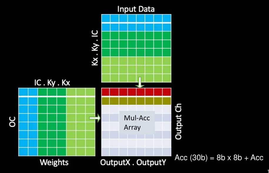
The MAC Array
The main operation of CNNs are of course convolutions which account for 98.1% of all the operations the Tesla software executes on the NPU with deconvolutions accounting for another 1.6%. The vast effort was spent on optimizing the MACs.
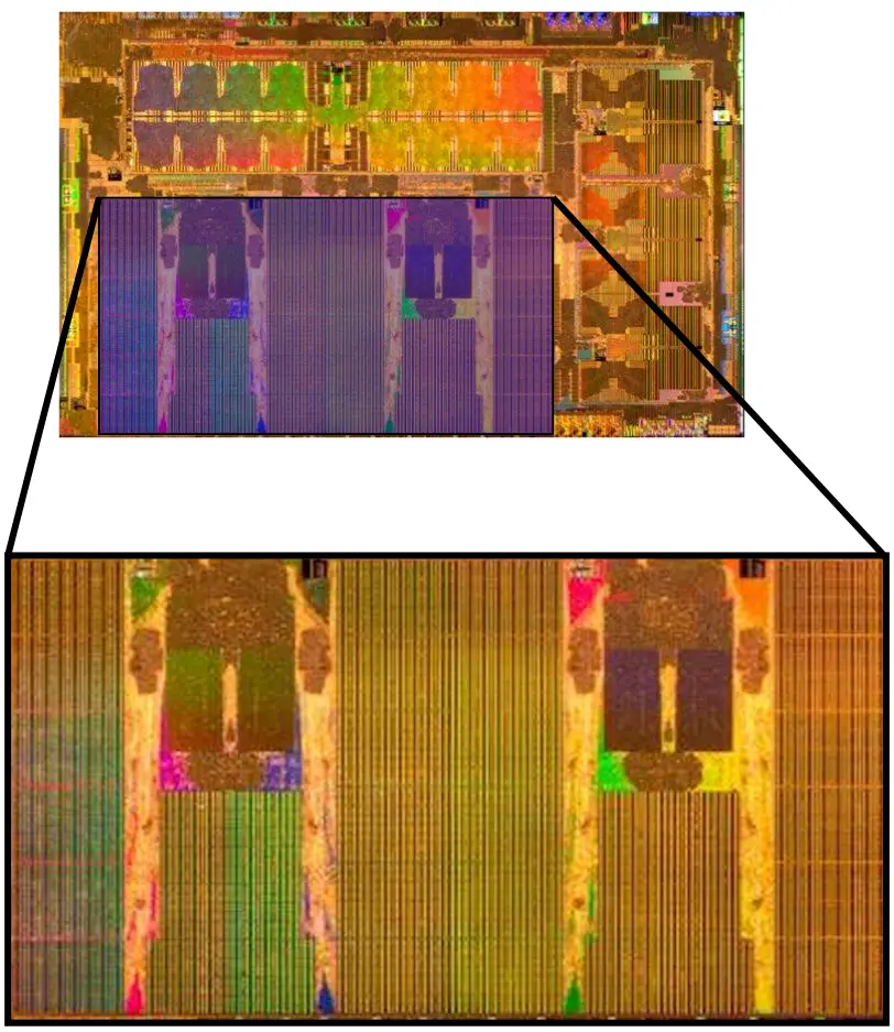
Data reuse in the MAC array is important, otherwise, not even a terabyte per second of bandwidth will suffice. In some designs, in order to improve performance, it’s possible to work on multiple images at once. However, because latency was a critical attribute of their design for safety reasons, they must operate on individual images as quickly as possible. Tesla does do a number of other optimizations here. The NPU operates on multiple output channels in parallel by merging the output pixels in the X and Y dimensions within an output channel. This allows them to parallelize the work and operate on 96 pixels at the same time. In other words, when they work on all the pixels in the channel, all the input weights are shared. Additionally, they also swap the output channel and input channel loops (see the code segment in the photo below). This allows them to work on all the output channels sequentially, sharing all the input activation without further data movement. It’s another nice reduction in the bandwidth requirements.

With the optimizations mentioned above, the MAC array operations are simplified. Each array comprises 9,216 MACs and is arranged in a 96 by 96 cells of independent single-cycle MAC feedback loops (note that this is not a systolic array, there is no data shifting inter-cells). In order to simplify their design and reduce the power, their MACs comprise 8-bit by 8-bit integer multiply and a 32-bit integer addition. Tesla’s own models are all pre-quantized when they are sent to customers, so the chips just store all the data and weights in 8-bit integers.
Each cycle, the bottom row of the input data and the right-most column of the weights are broadcasted across the entire MAC array. Each cell independently performs the appropriate multiply-accumulate operation. On the next cycle, the input data is pushed down by a row while the weights grid is pushed to the right by a row. The process is repeated with the bottom-most row of the input data and the right-most column of the weights getting broadcasted across the array. The cells continue to independently perform their operation. At the conclusion of a full dot product convolution, the MAC array is shifted down a row of 96 elements at a time which is also the throughput of the SIMD unit.
The NPU itself is actually capable of running at over 2 GHz though Tesla quotes all the numbers based on a 2 GHz clock so presumably, that’s the production clock. Operating at 2 GHz, you get a peak compute performance of 36.86 teraOPS (Int8) per NPU. The total power consumption of the NPU is 7.5 W or roughly 21% of the FSD power budget. This puts them at a performance-power efficiency of around 4.9 TOPs/W which is one of the highest power efficiency we have seen to date in a shipping chip – in a tie with Intel’s recently-announced NNP-I (Spring Hill) inference accelerator. Albeit it’s a little questionable how general-purpose the Tesla NPU really is in practice. Note that with two NPUs on each chip, they consume slightly over 40% of the total power budget.
SIMD Unit
From the MAC array, a row is pushed into the SIMD unit. The SIMD unit is a programmable execution unit designed to provide Tesla with some additional flexibility. To that end, the SIMD unit provides support for things such as sigmoid, tanh, argmax, and various other functions. It comes with its own rich set of instructions which are executed by a slave command sequencer. The slave command sequencer gets its operations from the extensions slot of the instruction which was described earlier. Tesla says that it supports most of the typical instructions you’d find in a normal CPU. Outside of that, the SIMD unit is equipped with a piplined quantization unit capable of performing normalization, scaling, and saturation.
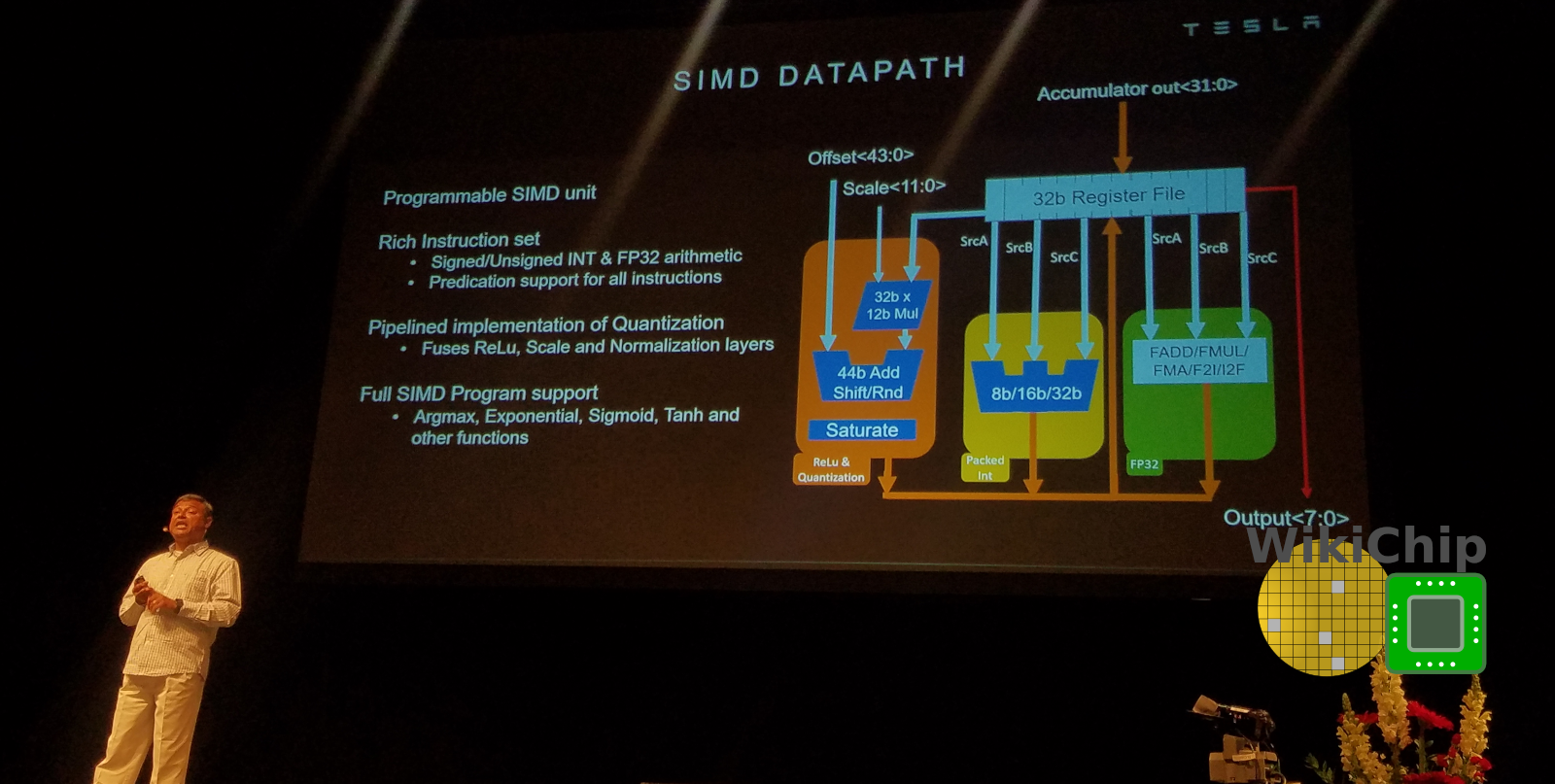
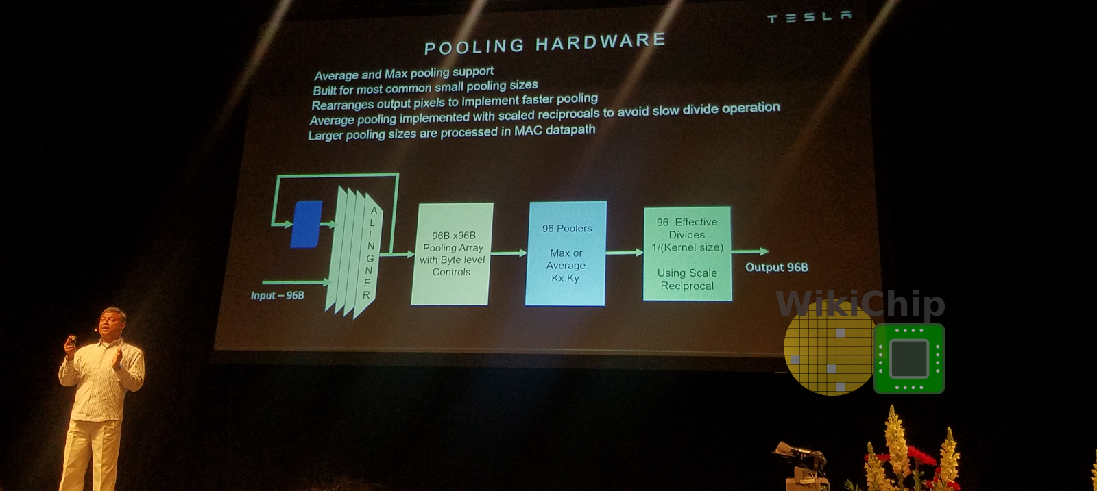
From the SIMD unit, results are forwarded to either the pooling unit, if needed, or directly to the write-combine where it is opportunistically written back to the SRAM at a rate of 128B/cycle. This unit does 2×2 and 3×3 pooling with higher-order being done in the conv unit. It can do max pooling and average pooling. For average pooling, the divide is replaced by a fixed-point multiplication unit using a constant based on either 2×2/3×3. Since Tesla initially interleaved the output channels for the MACs array, they do proper re-alignment first to correct for that.
All in all, Tesla achieved its performance goals. The FSD computer (HW 3.0) provides 21x performance uplift over the prior generation (HW 2.5) while raising the power by just 25%. The Tesla FSD Chips and FSD Computers are shipping today.
–
Spotted an error? Help us fix it! Simply select the problematic text and press Ctrl+Enter to notify us.
–