
ISSCC 2018: The IBM z14 Microprocessor And System Control Design
System Control (SC) Chip
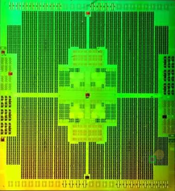
The system control chip serves two unique purposes: it facilitates the drawer-to-drawer connectivity and it contains the L4 cache. Like the CPU, the SC chip is also fabricated on 14HP and runs at 2.6 GHz. Containing 9.7 billion transistors on a massive 696 mm² die, the chip has 21.7 kilometers of wire and roughly 20,000 C4s.
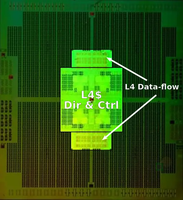
In the center is the L4 directory and control logic. The L4 directory consists of 160 MiB of eDRAM. To the bottom and top of the directory is the L4 data-flow logic. All data flowing from the I/O ports to the L4 caches go through that unit.
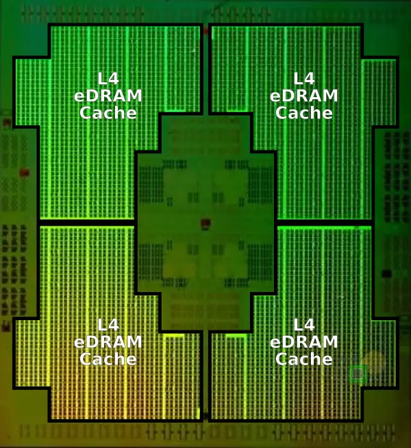
Surrounding the directory and control are four slices of 168 MiB of L4 eDRAM cache for a total of 672 MiB.
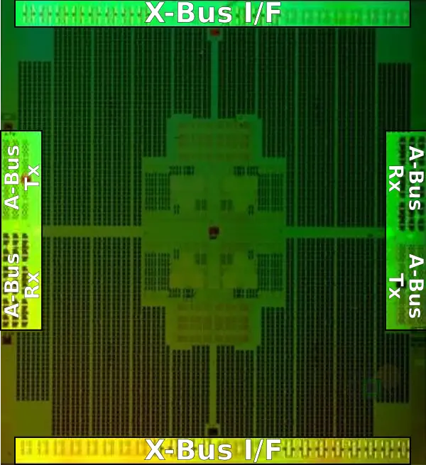
To the left and the right of the caches are the A-bus links. The A-bus links are the interconnects that go from one SC chip to another SC chip for drawer-to-drawer connectivity. The A-bus links use differential pairs with 7.8 Gb/s bandwidth per lane for 670 Gb/s bandwidth per link for a total of 2 Tb/s of drawer-to-drawer bandwidth. On the top and bottom of the die are the X-bus interfaces. Those links are single-ended interfaces running at 5.2 Gb/s per lane for 800 Gb/s per link for a total of 4.8 Tb/s of CP-SC bandwidth.
DT Gradient, Variations, and Yield Problems
The transition to a new process technology is not without risk. IBM’s transition to 14nm resulted in unique problems that needed to be addressed. One of the unique features of this 14nm FinFET on SOI process is its deep trench (DT) structures. Those very deep structures, around 3 microns in depth, can create large physical stresses on the wafer. The localized planar distortions worsen the gate height and CMP process controls.

In practice, the die comprises areas with eDRAM with high DT density (around 10%) and non-eDRAM areas with low DT density (around 1%). The large difference in DT density results in significant variations in performance. A special process was developed to perform DT density gradient analysis across the entire design, locating areas with low DT density and high DT density in order to detect possible problems.
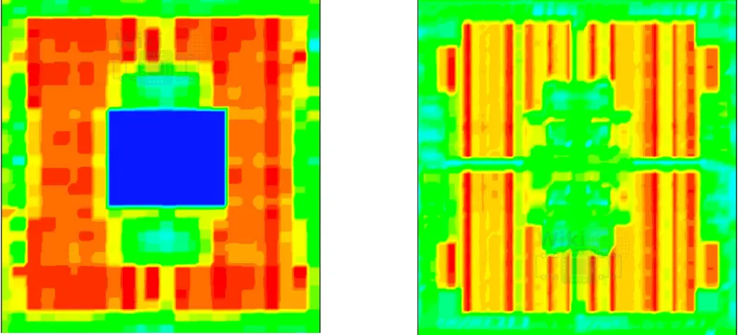
In the original SC chip design, SRAM was used for the L4 directories. This created a situation where the surrounding L4 eDRAM caches consisted of mostly high-density DTs while the central area, which was mostly SRAM, consisted of low-density DTs. The die image below on the left is the original SC chip with the blue area consisting of low-density DTs. The DT gradient variations in that design led to near-zero yield in hardware. Major modifications were needed in order to reduce the distortions. One of those changes included swapping the SRAM in the directories to eDRAM to reduce the gradient across the design. The changes to the caches and directories can be seen picture on the right. The final design had a more uniform DT baseline across both eDRAM areas and non-eDRAM areas which resulted in acceptable distortion/yield projections.
–
Spotted an error? Help us fix it! Simply select the problematic text and press Ctrl+Enter to notify us.
–