Intel Process Technology And Packaging Plans: 10nm in June, 7nm in 2021
An outline of Intel’s process technology and packaging plans including their 10nm and 7nm nodes as discussed at the company’s recent investor meeting.
Read more
Your Chips and Semi News
An outline of Intel’s process technology and packaging plans including their 10nm and 7nm nodes as discussed at the company’s recent investor meeting.
Read more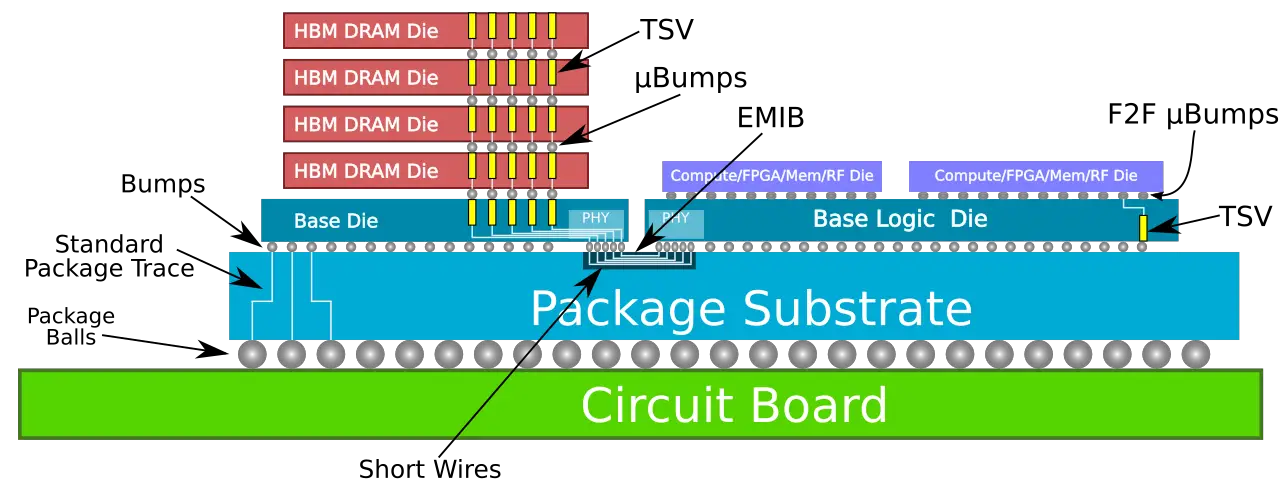
At the recent Intel Architecture Day, the company unveiled their latest advanced packaging technology called Foveros, a face-to-face three-dimensional (3D) die stacking packaging technology in an effort to assist with the slowing of Moore’s Law.
Read more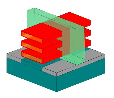
Samsung gives an update on their 7nm EUV-based process, details the foundry technology roadmap down to 3nm and the ARM ecosystem that follows.
Read more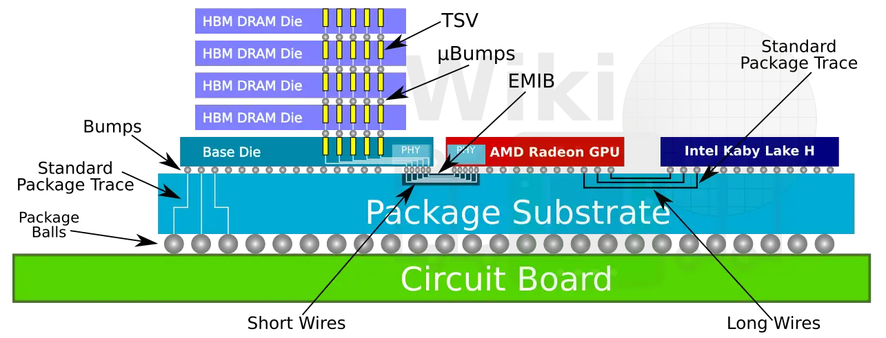
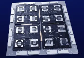
A look at Intel’s current generation of Thin & Light processors with high-performance graphics, formerly known as Kaby Lake G, from Hot Chips 30.
Read more