Intel Axes Nervana Just Two Months After Launch
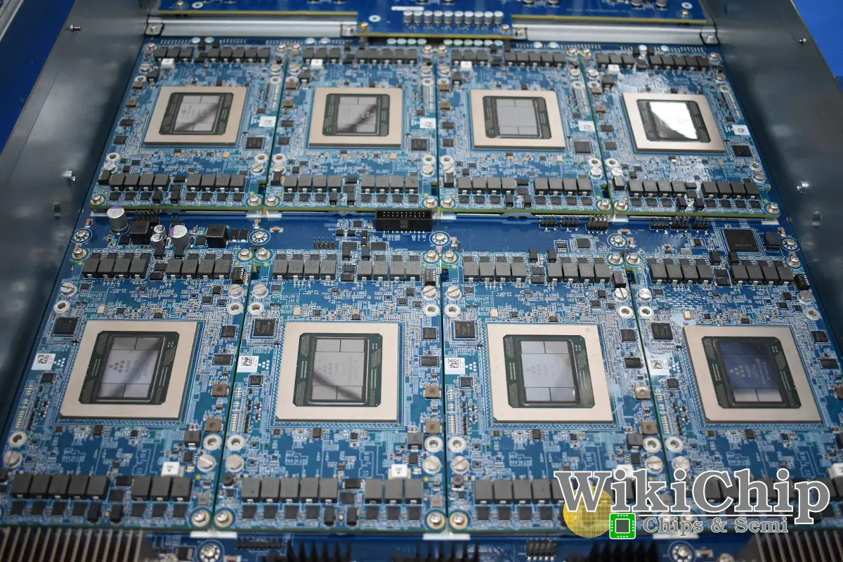
In a low-key announcement, last Friday Intel announced that it decided to cease all further development on its Nervana Neural Network Processor for training line. The move comes just two months after the much-delayed Nervana NNP family launched.
The announcement itself isn’t very surprising. In mid December the company announced its acquisition Habana Labs for approximately $2 billion. With two AI companies designing two architecturally very different chips for the very same markets, it was just a matter of time before one had to get axed. For the time being, it looks like the Intel NNP-I will continue for a little longer due to customer commitments but will eventually discontinue in favor of the Habana chips. Recently, Intel also announced 3rd generation Movidius VPUs, codename Keem Bay. To that end, Intel has confirmed that there are no changes to the Movidius roadmap for vision processing.
The official statement from Intel is published below.
Changes to Intel AI Data Center Accelerator Roadmap
After acquiring Habana Labs in December and with input from our customers, we are making strategic updates to the data center AI acceleration roadmap. We will leverage our combined AI talent and technology to build leadership AI products.
We will bolster the current and next generation of Habana Goya and Gaudi with Intel’s AI hardware and software innovations. The Habana product line offers the strong, strategic advantage of a unified, highly-programmable architecture for both inference and training. By moving to a single hardware architecture and software stack for data center AI acceleration, our engineering teams can join forces and focus on delivering more innovation, faster to our customers. As part of this update we plan to deliver on current customer commitments for the Intel NNP-I inference accelerator (code-named “Spring Hillâ€) and cease development of the Intel NNP-T (code-named “Spring Crestâ€).
This roadmap decision aligns to Intel’s AI Strategy and our commitment to deliver heterogeneous AI solutions that fit our customers’ evolving power and performance needs – from the intelligent edge to the data center.
Comparison
The discontinuation of Nervana and the adaptation of Habana is a puzzling move for us. We have been struggling to justify it on technical grounds. For the most part, at least on paper, Nervana’s architecture is superior in terms of future scalability (future nodes and advanced packaging perspective) and in terms of workload capabilities. Specifically, Spring Crest should do better in terms of workload parallelism, especially massive scale-out parallelism.
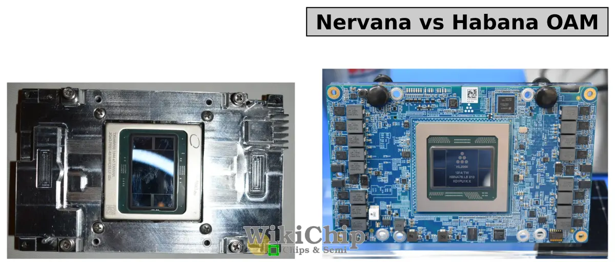
First, let’s look at the complete product. The Nervana products are sold under the NNP brand while Habana HL Series. For training, both Nervana and Habana offer a PCIe card and an OAM mezzanine module.
| SKU Comparison | ||||
|---|---|---|---|---|
| Company | Nervana | Habana | ||
| SKU | NNP-T 1300 | NNP-T 1400 | HL-200/202 | HL-205 |
| FF | PCIe Card | OAM Module | PCIe Card | OAM Module |
| TDP | 300 W | 375 W | 200 W | 300 W |
| Memory | 32 GiB HBM2 |
32 GiB HBM2 |
32 GiB HBM2 |
32 GiB HBM2 |
| Bandwidth | 1.23 TB/s | 1.23 TB/s | 1.02 TB/s | 1.02 TB/s |
| Scale-out | 16×112 Gb/s ICLs | 16×112 Gb/s ICLs | 8×100 GbE | 10×100 GbE |
So far everything is pretty much the same. Every chip in the table above comes with 32 GiB of HBM2 memory. Nervana chips have slightly higher TDPs and higher clocked memory but generally have much lower actual typical power consumption. Nonetheless, high-level packaging decisions are very similar. The real difference, of course, is in the implementation. We won’t touch on every aspect of the implementation (for that, feel free to visit our detailed Spring Crest and Gaudi pages) but point out some of the key differences.
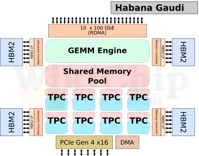
On the implementation side, Gaudi and Spring Crest are vastly different. Gaudi can be described by its three major components – the GEMM engine, the shared memory, and the eight Tensor Processing Cores (TPCs). Unfortunately, Habana withheld a number of critical pieces of information to make a proper comparison. We have taken the liberty to guesstimate some of those values. The TPCs are Habana’s custom VLIW SIMD DSPs. Each of those cores supports 8-bit, 16-bit, and 32-bit SIMD vector operations for both integer and floating-point. There is also support for bfloat16. There are eight of those on the die. For deterministic reasons, there are no caches but there is a small slice of local SRAM with each TPC. Habana did not disclose the size of the local memory but on a 16 nm 1-1.5 MiB isn’t unreasonable.
The other part of the compute in Gaudi is the General Matrix Multiply (GEMM) engine. The engine operates on 16-bit integers. Habana did not disclose much about the implementation behind this GEMM engine but there has been speculation that it was inspired by Google’s TPUs. Google stuck with a systolic array of 128×128 in size (implementing multiple such instances on the same chip). It’s not unreasonable to expect Habana to feature a similarly-built GEMM engine. A similar architecture (128×128) at 1.2-1.5 GHz will peak at 50 teraFLOPS while a twice as large array of 256×256 at 1 GHz will peak at 131 teraFLOPS.
Both the GEMM engine and the TPCs share a large pool of memory. Habana did not disclose the size of this SRAM but we can speculate it’s a sizable amount, probably around 32-48 MiB of memory.
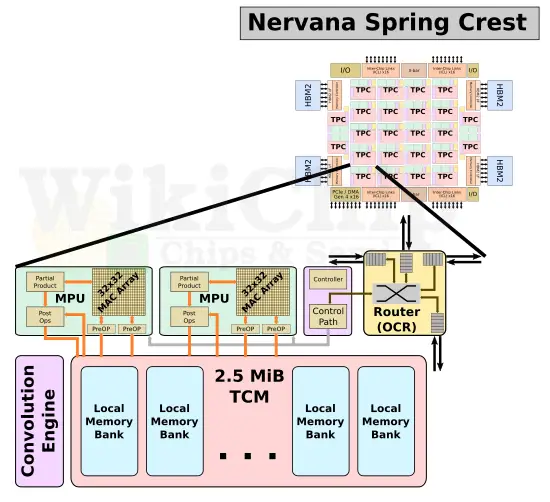
Nervana’s design, on the other hand, has a more complex design. Spring Crest implements a uniform 2D mesh of 24 tensor processor clusters (TPCs). Note that the ‘C’ in TPC here means cluster and not core. Each cluster comprises the on-chip router (OCR), the control, the MAC processing units (MPU), and the memory subsystem. There are actually two MPUs per cluster.
The processing unit comprises a large matrix multiply array as well as vector operations and specialized deep learning functions. The matrix multiply core is a 32×32 array that uses bfloat16 for the multiply and FP32 for the accumulate. Outside of the matrix core is the compound vector pipeline that can perform multiple operations on a set of inputs and intermediate values intended to lower the effective memory bandwidth and power. Both FP32 and BF16 are supported throughout the entire compound vector pipeline.
Each TPC contains 2.5 MiB of local scratchpad memory. With a total of 24 TPCs, there is 60 MiB of scratchpad memory in total on-die. The memory is highly-banked and multi-ported, designed for simultaneous read and write accesses. As part of the memory ports, there is native tensor transpose support. This means tensor transpose can be done directly by simply reading and writing into memory without any additional overhead.
| Intel Nervana Spring Crest | |
|---|---|
| TPCs | 24 |
| Local Memory | 2.5 MiB/TPC |
| Total Memory | 60 MiB |
| HBM | 32 GiB |
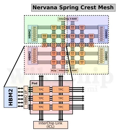
All 24 TPC instances are interconnected using a 2D mesh. Nervana spent considerable effort into ensuring data remains localized, reducing data movement and improving reuse. This makes their design particularly advantageous from a future improvement point of view. In fact, Nervana themselves scaled nicely the number of TPCs from 12 to 24 going from their first-generation Lake Crest (which was never productized) to Spring Crest. Spring Crest is physically partitioned into four PODs. Within each pod are six TPCs. Each pod is connected to its own, physically nearest, HBM stack and external InterChip interconnects (ICLs), and to neighboring pods.
Parallelism is baked directly into the architecture which, at least on paper, should enable very good scaling. The 2D mesh is no exception. There are actually a total of three full-speed bidirectional meshes – for the HBM, external InterChip interconnects, and neighboring pods. The dedicated buses are designed to reduce interference between the different types of traffic. It’s worth noting that the Nervana software stack has control over much of this – capable of explicitly managing to optimize data locality and data residency. This applies to both the on-die memory and the off-die HBM memory, and by an extension when scaling-out can be used to carefully orchestrate more optimal allocations of resources for chip-to-chip traffic as well.
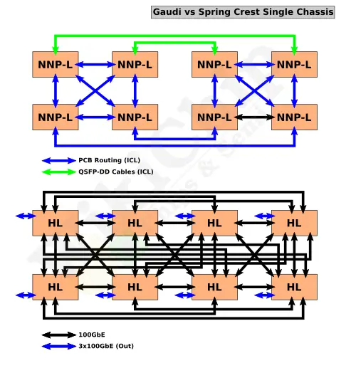
The scale-out differences are also interesting. Habana went with a more straightforward approach. Here, Gaudi implements 10×100 GbE (or 20×50). The reason they are given is that they wanted to leverage the large existing Ethernet hardware base. It’s also entirely possible they simply didn’t have the resources to develop something more ambitious. This interface also integrates RoCEv2 on-die, thereby providing a glueless RDMA over Converged Ethernet solution (without a NIC). Nervana developed its own propitiatory InterChip Link (ICL) which comes with a fully programmable router built-in and supports virtual channels and priorities for traffic management and deadlocks avoidance as well as support glueless complex topologies such as ring, hybrid cube mesh, and fully connected. There are 16 ICLs per chip. They are grouped into four ports of quads, each with a peak bandwidth of 112 GB/s for a total peak aggregated bandwidth of 448 GB/s (3.584 Tb/s).
| Scale-out Capabilities | ||
|---|---|---|
| Company | Nervana | Habana |
| Microarchitecture | Spring Crest | Gaudi |
| I/O | 16×112 Gb/s ICLs | 10×100 GbE |
Although Spring Crest could scale to many racks gluelessly, a source has suggested to WikiChip that Intel was also working on an ICL switch to allow further flexibility. There are no scaling benchmarks from Habana but pre-production silicon from Nervana showed very good scaling utilization across 100s of nodes with very low latencies even at sizable transfer sizes.
Why Switch?
No independent benchmarks on either company have been published therefore we can only go with what we know. On paper, Nervana’s architecture is superior. It’s hard to see why Intel chose Habana over Nervana based on technical merit. The official statement from Intel suggests that the Habana unified architecture is a “strategic advantage” but that’s questionable at best. We didn’t touch on Habana’s Goya which is their inference architecture. Goya is identical to Gaudi with the exception that the HBM interfaces are replaced by standard DDR4 interfaces. That’s a bonus, but consider this. While Intel’s NNP-I, codename Spring Hill, (the inference version of NNP-T) is, in fact, an entirely different architecture to Spring Crest, it largely builds on Intel’s own mobile client SoC. For their first-generation, Spring Hill shares almost everything with Ice Lake. Spring Hill engineers explained that the shared architecture with Ice Lake significantly simplified development and expedited time-to-market. That’s essentially the claim Intel is making with the switch to Habana.
Beyond hardware, it’s also entirely possible that the problem boiled down to software. First-generation Nervana NNP’s (Lake Crest) encountered software-related difficulties primarily due to using the Flexpoint data type. Spring Crest pivoted away from Flexpoint in favor of bfloat16 which Nervana claimed easied software development. Since the first SKUs just started shipping, it’s really hard to tell whether software really killed Spring Crest. Perhaps the easiest way to explain this move is from the first sentence of the official statement which suggests Habana received the likes of certain, presumably large, customers (we know Facebook was one). Whatever the real reason for the switch may have been, it’s not at all obvious from an external observer point of view. Ultimately, the best architecture doesn’t necessarily win and maybe Habana will more easily allow Intel to gain market share in the growing AI ASIC market. Only time will tell if this critical decision was the correct one.
–
Spotted an error? Help us fix it! Simply select the problematic text and press Ctrl+Enter to notify us.
–

