
Arm Ethos is for Ubiquitous AI At the Edge
Leading mobile SoC designers have been integrating dedicated NPUs in their SoCs for a number of years. Late last year Arm announced the Ethos NPU family. The move is Arm’s latest effort to expand into the AI market. Arm is coming into the market with a commercial solution a good bit behind most custom SoC designers and this is expected due to the vast number of customers and the scope they have to cover with just a limited number of NPU IPs.
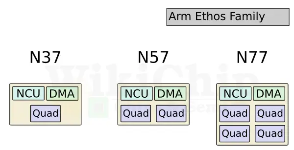
The company launched three initial IPs under the new Ethos NPU family. The three initial IPs are designed to cover quite a large spectrum of devices. The Ethos-N37, the Ethos-N57, and the Ethos-N77. As their names imply, each one is increasingly more powerful than the previous one.
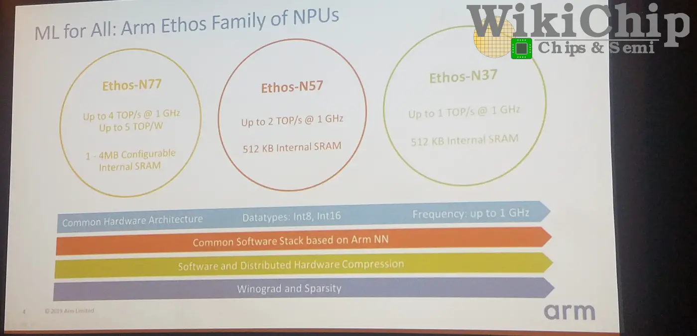
The three NPUs are built using the same microarchitecture but with slightly different configurations as you’ll see in a little bit. The visual graph by Arm below plots the various markets and constraints the NPUs are working within. At the low-end is the Ethos-N37 which targets devices with the lightest workloads with a peak compute performance of up to around 1 TOPS with very little DRAM bandwidth available around 3 GB/s or less. The Ethos-N57 covers more complex devices such as most of the smart home devices as well as some mainstream smartphone SoCs. The N57 is designed to work with higher memory bandwidth and deliver up to around 2 TOPS. Finally, there is the Ethos-N77. This is the top SKU in the stack targetting up to 4 TOPS with a relatively high power efficiency of around 5 TOPS/W. The N77 is designed for premium and possibly mid-range AR/VR devices, albeit for performance AR, you’ll need something a bit more powerful. For higher performance higher memory bandwidth is required. To get to the highest performance, the memory bandwidth needs to be as much as 8 GB/s or even higher. It’s worth pointing out that there is a good amount of overlap between the three IPs. The N57 can cover the upper part of N37 range as well as the lower half of the N77 range. Same with the N77. This is to give SoC designers some wiggle room as to how they want to go about their design.

What’s powering the new Ethos family of NPUs is Arm’s ML Processor (MLP). We will only be touching the key design points in the article. If you are interested in the full microarchitectural information, as usual, have a go at our main MLP article.
 Machine Learning Processor (MLP) – Microarchitectures – ARM
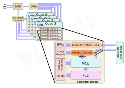
At the heart of the Ethos family is Arm’s ML Processor (MLP). MLP is a clean-sheet ground-up microarchitecture for the acceleration of machine learning – with emphasis on CNNs and RNNs. The MLP actually uses a fairly straightforward design which is what we would expect from an IP that sold to designers to be integrated into all kind of SoCs. At a high level, the MLP main components are the control unit, the DMA, the broadcast network, and the compute engines. As you might have guessed, the main action takes place in the compute engines. Each cluster of four compute engines are grouped into a ‘quad’. The control unit orchestrates the entire execution of the neural network across the compute engines as well as the DMA engine which understands the neural network mapping and can ensure data arrives when needed.
The MLP can be implemented in a number of various configurations. The two main control knobs are the SRAM bank sizes within each compute engine and the number of compute engines. For their current design, the MLP can have anywhere from a single compute engine in a single quad and all the way to four quads with sixteen compute engines. Within each compute engine you have a chunk of SRAM which stores the input and output feature maps and the weights. It can be configured from 64 KiB and all the way to 256 KiB. Regardless of the configuration, the control unit and the DMA are always the same.
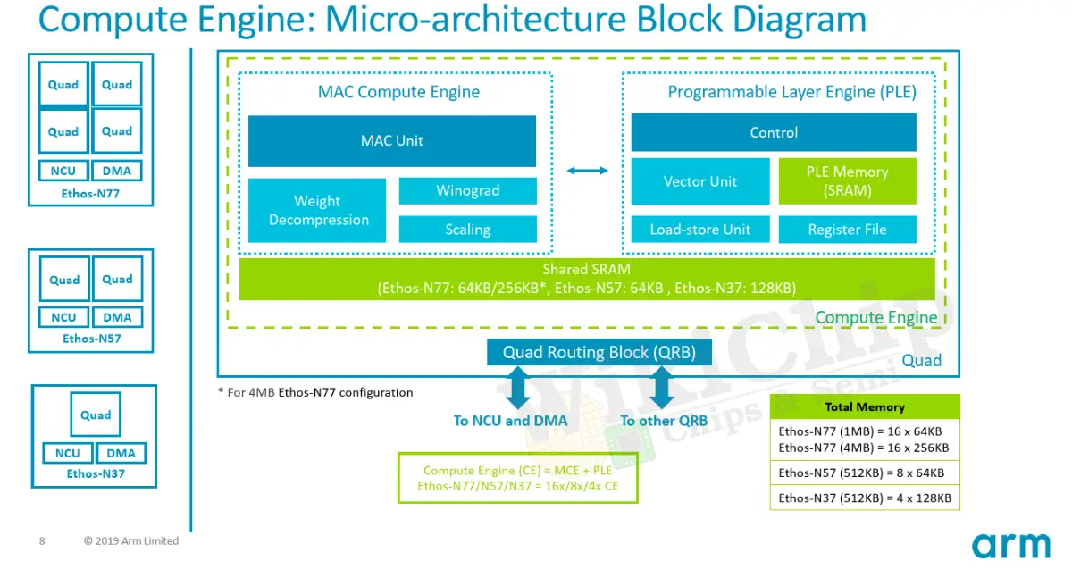
The Ethos-N77 is essentially the full MLP configuration. It features four quads with 16 compute engines with two possible SRAM configurations – either 64 KiB or 256 KiB. Likewise, the Ethos-N53 incorporates four quads for a total of eight compute engines. The N53 comes with a fixed 64 KiB SRAM bank per CE. The lowest performance SKU, the Ethos-N37 has a single quad for a total of just four compute engines with fixed 128 KiB capacity SRAM banks.
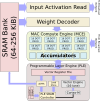
The two interesting components within the compute engines are the MAC Compute Engine (MCE) and the Programmable Layer Engine (PLE). The MCE contains the high-efficiency fixed-function MAC units while the PLE contains the flexible programmable vector engine. The flow is relatively simple. An input activation tensor along with the weights are passed to the MCE. Following the computation, results are passed to the PLE for post-processing and various other operations that might be needed. There is not complicated control because much of it was thrown onto the compiler which performance static scheduling, pre-partitions the SRAM banks, and compresses the feature maps and the weights.
Within the MCE are a set of eight MAC units. Each MAC unit is 16 wide. In other words, each MAC unit can do 16 8-bit dot product operations each cycle. In total, you are looking at 256 OPs/cycle of peak performance per compute engine. By the way, operations here are all 8-bit wide with a 32b accumulate. The MLP does support 16-bit operations but it’s going to cost you a 4x reduction in throughput (i.e., 64 OPs/cycle). The peak theoretical performance for each of the Ethos SKUs is listed in the table below. Of course, the real workload performance will depend on the utilization of those MACs. One thing to point out is that all three SKUs can reach the same max frequency of 1 GHz.
| Arm Ethos NPUs | |||
|---|---|---|---|
| SKU | N37 | N57 | N77 |
| Quads | 1 | 2 | 4 |
| CEs | 4 | 8 | 16 |
| Max Frequency | 1 GHz | 1 GHz | 1 GHz |
| SRAM Banks | 128 KiB | 64 KiB | 64 KiB 256 KiB |
| Total SRAM | 512 KiB | 512 KiB | 1 MiB 4 MiB |
| OPS | 1024 OPs/clk | 2048 OPs/clk | 4096 OPs/clk |
| Performance | 1.024 TOPS (Int8) 256 GOPS (Int16) |
2.048 TOPS (Int8) 512 GOPS (Int16) |
4.096 TOPS (Int8) 1.024 TOPS (Int16) |
While the N77 tops out at 4.1 TOPS, an actual SoC need not max out at that performance level. Instead, multiple instances of the MLP can be integrated onto the SoC in order to increase the performance further. So for example, there is support for tiling using the CCN-500 interconnect to scale to up to eight MLPs or the newer CMN-600 mesh interconnect to scale to even 100s of MLPs – at least in theory.
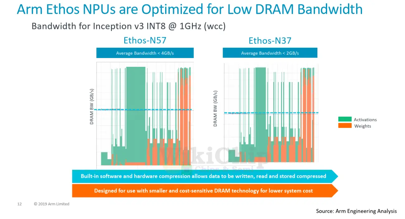
In addition to the MCE, the other main component within the compute engine is that Programmable Layer Engine (PLE). The PLE is actually more powerful than the MCE and is far more flexible because it’s programmable, albeit it loses out in a raw power-efficiency competition when dealing with millions of repeated MAC operations. The PLE is a full-fledged Cortex-M processor with the vector and NN extensions baked into it. And yes, if you are wondering, it does, in fact, mean the Ethos-N77 incorporates sixteen of those Cortex-M vector processors internally. It’s designed with a dedicated 16-lane vector engine coprocessor model. The PLE is mainly designed to do the post-processing from the MCE as well as implement some of the less common functions. But since this is a highly capable vector engine in itself, it can in effect operate directly on the SRAM data with and without the assistance of the MCE. The programmability of the PLE allows the Arm software team to quickly adapt to new AI models and functions. The compiler toolchain does a number of other optimizations we have come to expect from contemporary NPUs. Since the compiler partitions the SRAM ahead of time, it performs activation and weights compression which helps reduce the bandwidth a bit across the entire design. Additionally, there is light optimization for sparsity. Data paths will be gated on zeros, saving a little on power.
–
Spotted an error? Help us fix it! Simply select the problematic text and press Ctrl+Enter to notify us.
–