
TSMC N3, And Challenges Ahead
In the relentless quest for smaller and more power-efficient transistors, the semiconductor industry has encountered amplified challenges, which recent cutting-edge process nodes have brought to the forefront. TSMC’s newest node is its 3-nanometers “N3” process technology family. Initially planned for a mass production ramp in the second half of 2022, TSMC finally held a 3-nanometer volume production and capacity expansion ceremony on December 29th, 2022 at their Fab 18.
N3
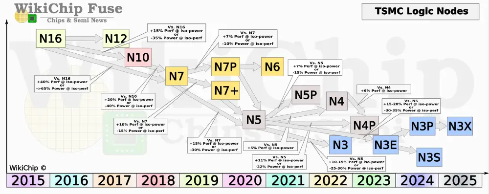
As we detailed in a previous article, TSMC is rolling out a number of “3nm” flavors. The two primary flavors are a Base N3 node (N3B) and an Enhanced N3 node (N3E). Most recently, at their 2023 Technology Symposium, the company announced a number of additional derivative nodes as well. However, despite their names, the two are not related and follow wildly different design rules. For all intents and purposes, we will treat them as two separate lineages. TSMC also plans on introducing a number of higher-performance variants of the N3E later on.
At the 68th Annual IEEE International Electron Devices Meeting (IEDM), TSMC presented a number of papers – two for their N3 nodes. The second paper was actually a “late-news submission”. Though not spelled out in the paper, we did confirm with the author that the first paper refers to N3B while the second paper is their N3E node. At the TSMC 2023 Technology Symposium which was held last month, TSMC disclosed a number of additional details that were not disclosed previously. We will be detailing it all here.
N3B
The initial 3-nanometer class process technology, N3B has recently entered mass production. Although TSMC continued with its recent tradition of disclosing a very minimal amount of actual details regarding its process, this paper was undoubtedly better than the N5 one from a couple of years ago. Here TSMC disclosed that the node features a contacted gate pitch of 45 nanometers, the tightest pitch reported to date by any foundry. It’s worth pointing out that, historically, TSMC relies on a slightly more relaxed CPP for their standard cell implementations. That puts N3B somewhere 45-47 nm for the CPP in real-world implementations.
One of the things TSMC introduced with their N3B node is a new self-aligned contact (SAC) scheme. This one surprised us since we thought they would have already introduced it by now. By comparison, Intel introduced SAC at their 22-nanometer process along with their FinFET transistor architecture all the way back in 2011. Samsung also introduced SAC a while back in their 7-nanometer family.
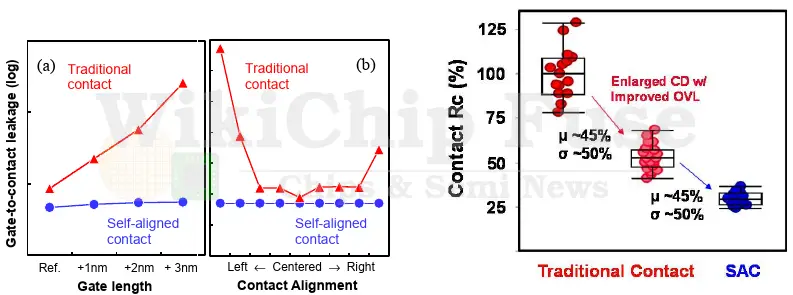
One of the many challenges that process engineers face when shrinking transistors is variations due to misalignments. On modern nodes, due to the small contact landing area, the margin for misalignment drops significantly, affecting yield. Beyond contact-to-gate shorts, parasitic capacitance and performance issues as a result also occur. To alleviate the issue, TSMC says that with their N3B and beyond, they have to introduce SAC. SAC – or self-aligned contact – is strictly a yield-improving flow that guards the gate against contact shorts due to the tight pitches in leading-edge process nodes.
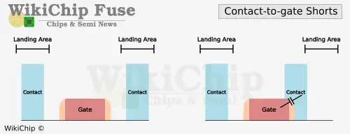
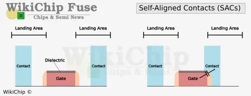
Under SAC, the gate is guarded against shorts through a dielectric hard mask on top of the gate. It also allows the contact to fully utilize the space adjacent to the spacers. The end product is a process flow that is much more forgiving with respect to process variations. It’s worth noting that the process does have the effect of worsening capacitance due to the proximity of the contact under misalignments.
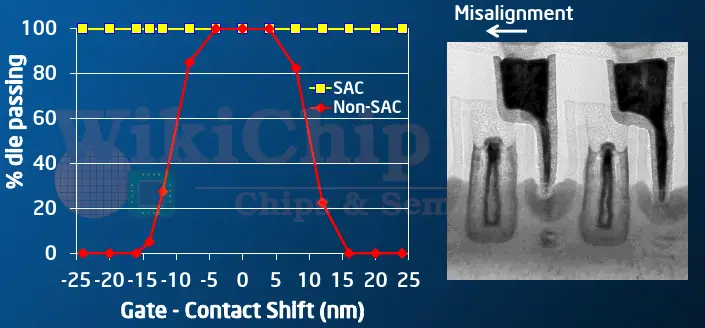
The graph below from TSMC shows how the SAC successfully suppressed the contact-to-gate leakage. Up to 3 nanometers in either direction is shown to have minimal impact on leakage when compared to a non-SAC variation. TSMC also reported SAC reducing resistance by 45% and variations by 50% versus a traditional contact scheme.
By the way, TSMC results for 3 nm are very similar to Intel’s 22 nm from 2012. Below is a slightly different graph from Intel for SAC on their 22 nm node which shows misalignment tolerances of up to 5 nm with 100% of the dies passing.
TSMC also talked a bit about spacer engineering. As the spacer thickness increases, and contact distance is reduced, contact resistance grows sharply. Therefore, reducing the spacer thickness is paramount to keeping the resistance within acceptable tolerance. It does so by lowering the gate capacitance to source/drain regions of the fins and to contact at the top. While thinner spacers are more desirable, they are difficult to implement as it adversely affect both the yield and reliability of the device (this is especially true for FinFET devices).
To that end, TSMC says it had identified and implemented a Low-K spacer with a K-Value < 4.0 suitable for mass production. In their N3B process, TSMC reported an up to 230 mV Vmax improvement over the previous spacer implementation while passing TDDB specs.
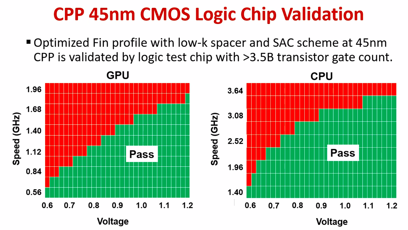
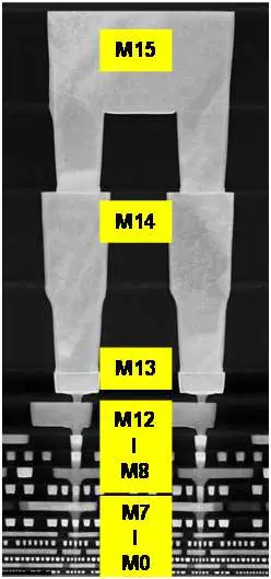
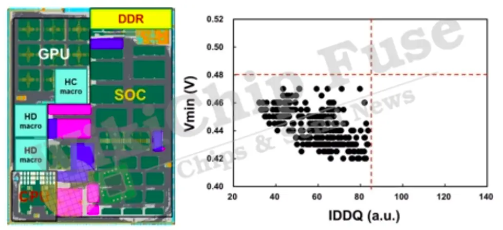
The same test chip also integrated 256 Mib of HC and HD SRAM macros.
N3E
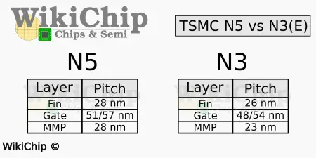
The N3E node is an entirely different process node TSMC plans on introducing in the second half of this year, roughly a year after the N3B introduction. This will be ‘The’ N3 node for the majority of customers. Everything about this node is different from N3B. To that end, the N3E node offers a 48-nanometer poly pitch, a 26-nanometer fin pitch, along with a minimum metal pitch of 23 nanometers. This represents a 0.94x and 0.93x scaling respectively.
To facilitate a 23 nm pitch minimum metal pitch, TSMC said it incorporated an “innovative liner for Cu” in order to reduce RC by 20% for nominal metal width and as much as 30% for 2x metal widths. Similarly, TSMC said that an “innovative barrier process” was used to reduce the Via RC by as much as 60%. Intel, by comparison, is using an enhanced Copper (eCu) which comprises a Tantalum barrier with Cobalt cladding surrounding a pure Copper core.
At the upper metal layers with more relaxed pitches, the barrier thickness was said to have been reduced and extreme low-κ dielectric was used to minimize overall BEOL RC delay.
A number of additional process features were briefly mentioned. This is a 6th generation high-K replacement metal gate process. For this process TSMC said it had improved the spacer engineering which appears to be similar to the one detailed for N3B. TSMC also mentioned the use of a raised Source/Drain with dual epi process which was optimized for channel strain for the purpose of reducing source/drain resistance.
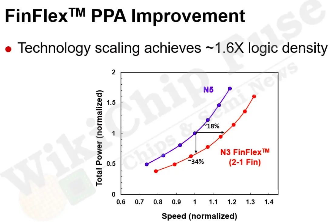
A large focus of TSMC N3E IEDM paper was “FinFlex” (hybrid cells) which the company describes as “an innovative standard cell architecture with different fin configurations.” As usual, TSMC developed, among other things, three main logic standard cell libraries – Short Height, Medium Height, and a Tall standard cell library comprising 1, 2, and 3 fins heigh cells respectively. In addition to their standalone applications, FinFlex offers three pre-defined configurations whereby those libraries are mixed together to provide various density-performance tradeoffs. In a way, FinFlex can be thought of as a fixed double-height standard cell but TSMC did combine them in a clever way to take advantage of the higher performance where needed and higher density where the performance is not essential.
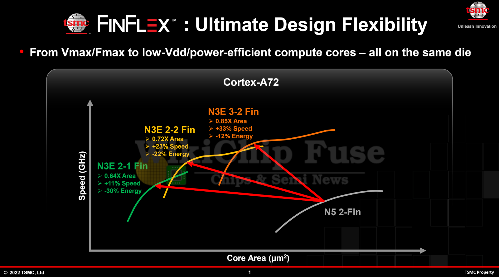
All three FinFlex variants utilize the medium-height, 2-fin, standard cells. TSMC says this was chosen due to its best performance-density balance. When combined with a 1-fin library (called a “2-1 Fin Configuration”), TSMC says it can achieve good area reduction without sacrificing performance for power-sensitive applications. Here, the 2-fin device within the hybrid setup can be used in critical paths to leverage higher currents while the single-fin cells are used for leakage reduction. TSMC says this produces the highest-density hybrid standard cells to date while offering the lowest power consumption. Likewise, when combined with a 3-fin library (called a “3-2 Fin Configuration”), the three-fin cells are used for higher drive currents for high-performance applications.
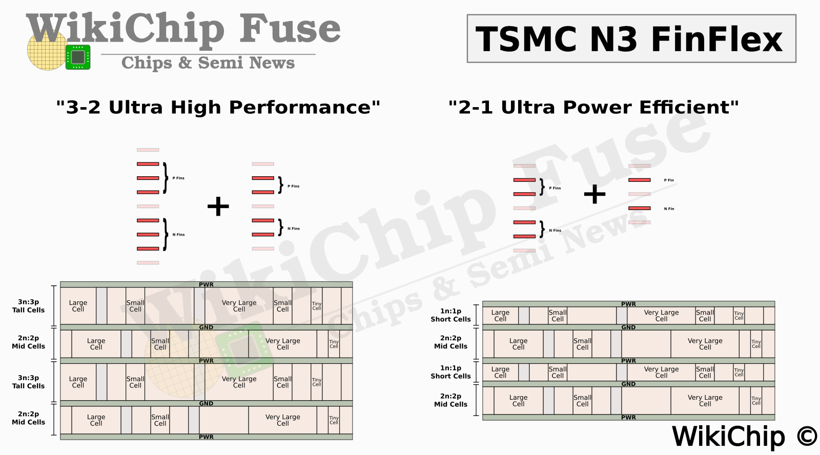
TSMC noted that with the hybrid cell FinFlex configurations, additional cell-level and chip-level capacitance reduction is achieved through co-optimization of BEOL place-and-route.
Putting this all together, the N3E cell heights are based on the 26-nanometers diffusion lines. Therefore, we have 4.5, 5.5, and 6.5 diffusion lines heights for the 1-, 2-, and 3- fin cells at the 48-nanometer CPP and 6.5, 7.5 and 8.5 lines height at the 54-nanometer CPP. This translates to 143-nanometers high-density cell heights at 48 nm CPP and 195-nanometers high density cells heights at the 54 nm CPP.
A 2-2 configuration at the 48nm CPP gives 286 nm hybrid cells as well as 390 nm at the 54 nm poly. This works out to 286 nm, 403 nm, and 455 nm at the 48 nm CPP and 390 nm, 559 nm, and 611 nm at the 54 nm CPP for 2-2, 2-1, and 2-3 respectively. Note this accounts for the extra H143/H195 that must be attached when in hybrid configuration.
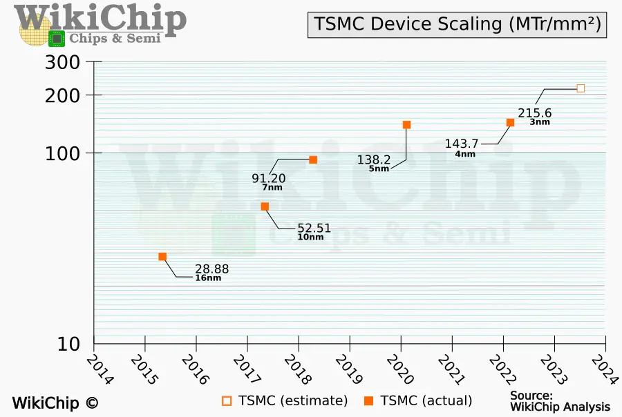
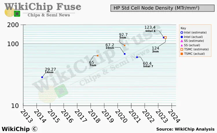
At a 48-nanometer CPP, the 143 nm HD cells give a transistor density of around 215.6 MTr/mm2.
This works out to about 1.56x transistor scaling in pure logic density (no analog/SRAM baked in, although those are essentially unchanged in this node) which is relatively closely to TSMC’s published number of 1.6x logic density based on 0.5[Logic]+0.3[SRAM]+.2[Analog] utilizing the 2-1 fin configuration.
At a 48-nanometer CPP, the 169 nm HP cells work out to around 182.5 MTr/mm2. The 3-nanometers high-performance cells (H221) with a 54-nanometer CPP produces a transistor density of around 124.02 MTr/mm2. Historically, we’ve only seen the high-density cells used with the relaxed poly pitch. That said, the 221-nm cells happen to be remarkably similar in density to the Intel 4 HP cells. The two are shown on the graph below for comparison.
In the context of 2-2, 2-1, and 2-3, the densities will work out to be an average of those depending on the configuration chosen. In terms of PPA, the 3-2 configuration is said to delivery 10% additional performance over N5 2-fin compared to the 2-2 configuration while offering half the area reduction as the 2-2 configuration. Likewise, the 2-1 configuration is said to offer 8% additional area reduction over the 2-2 configuration versus the N5 2-fin while offering half the performance improvement.
SRAM
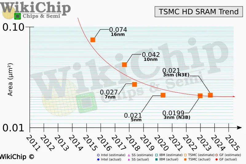
One interesting twist in the density story is SRAM. We wrote a piece about the collapse of SRAM scaling back in December. The bottom line here is that SRAM did not shrink on 3-nanometers while it simultaneously accounted for a larger portion of the die in terms of both absolute area and overall transistor count ratio. SRAM is a very important lever employed by chip designers used to improve performance, primarily through caching.
When TSMC first announced N3E, it left out its SRAM density improvement. We now know that the N3E SRAM bitcell is identical to N5. That’s a catastrophe for chip designers. N3B doesn’t fare any better. TSMC originally disclosed that N3B SRAM density was 1.2x over N5. A recent disclosure at IEDM revealed it’s actually a mere 5% more dense. N3B significantly higher price is hard to justify for the little added density and SRAM improvements.
PPACT
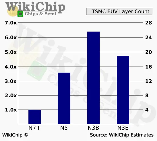
Recent process nodes have become increasingly intricate with a thousand steps. Apart from meticulous execution, the process design itself necessitates careful consideration of risk versus reward calculations. N3B was evidently intended to be a significant advancement over N5; however, this progress came at a considerable expense and extended time-to-market. At the lithography level, we estimated N3B to have bumped the number of EUV layers to 25. That represents a whopping nearly 80% increase. That’s an 80% increase in exposures, in litho total cycle time, and ultimately cost. It’s worth noting that N5 itself trippled the number of EUV layers from N7+. Clearly this trend is not sustainable even for another node.
N3B also introduced SAC. That is really peculiar to me, especially since it’s not present in N3E. The implications are that contacts were possibly double patterning initially – suggesting N3B might have topped 26 EUV layers – but was reduced to 25 under SAC enablement. The looser N3E pitch might have allowed them to get away without SAC altogether further reducing cost. N2 will most certainly make use of SAC in the future.
N3E took a huge step in reversing N3B costs. TSMC says that three critical layers that previously required double patterning were replaced by single EUV patterning. We take that to mean a total of 6 total – lines and vias – layers exposures were eliminated. This puts the estimated number of layers at 19. This suggests N3E a 36% intrinsic cost increase which is considerably more acceptable.
Many of the decisions made in N3 have likely made their way into TSMC’s future N2 node. We think that EUV layers in N2 will increase at a much modest rate compared to N3B, this is significantly more likely given that N2 is set to offer a new device architecture.
–
Spotted an error? Help us fix it! Simply select the problematic text and press Ctrl+Enter to notify us.
–