
IEDM 2022: Did We Just Witness The Death Of SRAM?
![]()
This year, the 68th Annual IEEE International Electron Devices Meeting (IEDM) was back in full force with nearly 1,500 engineers (in-person) from around the world making their yearly voyage back to downtown San Francisco to discuss the latest development in the semiconductor industry. While there were a great number of interesting papers from both academia and industry, it was the one by TSMC that brought frighteningly bad news – whereas logic is still scaling more-or-less along the historical trendline, SRAM scaling appears to have completely collapsed.
No Scaling!
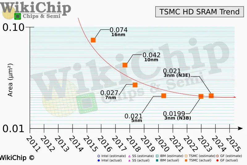
At the conference, TSMC talked about both the original base N3 (N3B) node as well as the enhanced variant (N3E) which is a slightly more relaxed variant of the N3B. What’s interesting is, for the new N3E node, the high-density SRAM bitcell size as not shrunk at all. Coming in at 0.021 µm², this is exactly the same bitcell size as their N5 node. The N3B variant which isn’t expected to make it into too many products did have a scaled SRAM bitcell; however, at 0.0199µm², it’s a mere 5% scaling (or 0.95x shrink).
In terms of rough memory density (assuming ISO-assist circuit overhead), N3E is roughly at 31.8 Mib/mm² and would increase to 33.55 Mib/mm² or 1.75 Mib/mm² (230 kilobytes) improvement.
Impact
That’s some seriously bad news! To put that into perspective, while N3B and N3E are both said to deliver a 1.6x and 1.7x chip-level transistor scaling, a 1.0x and 1.05x scaling of SRAM is catastrophic. Now, we still expect TSMC to roll out a denser SRAM bitcell variant for N3 at some point and we do expect to see some level of shrinkage for SRAM in the future, but the good old shrink SRAM shrinkage appears to be dead.
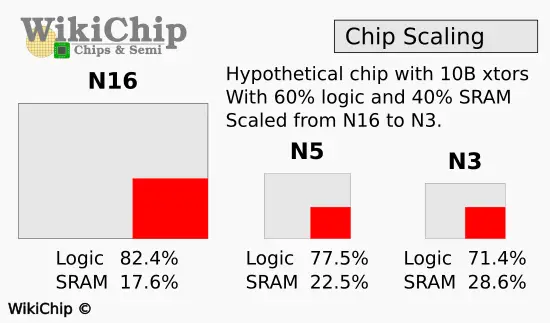
Consider a hypothetical 10-billion transistor chip comprising 40% SRAM and 60% logic in terms of transistor count on TSMC N16. Ignoring practical limitations and analog/phys/etc, such a hypothetical chip would have a die area of around 255 mm² with 45 mm² of it – or 17.6% – accounted for SRAM. Shrinking the exact same chip down to N5 would produce a 56 mm² chip with 12.58 mm² or 22.5% of the die accounted for SRAM. Shrinking the chip further to N3 (based on our initial – but not fully confirmed – values) would produce a 44 mm² chip with the same 12.58 mm² SRAM density which now accounts for nearly 30% of the area.
Of course, the impact won’t be felt the same across the board. The percentage of SRAM and caches on chips varies greatly by your target market and overall capabilities. However, for some AI hardware startups where the architecture dictates that a large portion of the chip be covered by SRAM, those engineers will encounter more challenges quicker than others.
Industry-Wide
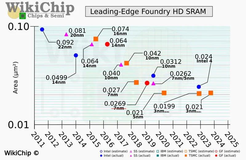
The collapse of SRAM scaling is not restricted to just TSMC. We have pointed out the slowing SRAM scaling issue for quite some time now. For example, while Intel is still shrinking its SRAM bitcells, the company’s most recently-announced Intel 4 process SRAM scaling slowed down to 0.7-0.8x scaling from their historical 0.5-0.6x scaling. For Intel 4, our estimated density (at ISO-assist circuit overhead vs TSMC) is at 27.8 Mib/mm² or 4 Mib/mm² or 13% behind. It would not be unrealistic to expect Intel’s Intel 3 process to match or beat them.
So where do we go from here? The reality is that currently, the only viable alternative to SRAM is simply more SRAM, and therefore we expect to see SRAM directly consuming more area. That’s not to say we don’t expect more SRAM scaling. While we do expect TSMC and other foundries to roll denser SRAM, it would appear that the historical scaling is officially dead. Some research institutions such as Imec presented higher-density SRAM bitcells. For example last year, at IEDM 2021, Imec presented SRAM densities of around 60 Mib/mm² or roughly twice today’s densities on a hypothetical “beyond 2 nm node” utilizing forksheet transistors and an advanced dual-sided interconnect scheme.
Beyond SRAM, the industry has been looking into many other alternative memory architectures. Emerging memory technologies include MRAM, FeRAM, NRAM, RRAM, STT-RAM, PCM, and others. Those emerging memory bitcells offer unique tradeoffs when compared to SRAM such as higher density at lower read/write specifications, non-volatility capabilities, lower read-write cycle capabilities, or lower power at potentially lower density or speeds. While they are not direct replacements for SRAM, moving forward they might play a role as level 4 or level 5 caches where the lower performance tradeoffs can be offset by higher density.
For now, it seems that the industry has reached an interesting inflection point.
Further Reading:
- N3E Replaces N3; Comes In Many Flavors
- A Look At Intel 4 Process Technology
- TSMC 2021 Foundry Update: Foundry Roadmap
- TSMC 2021 Foundry Update: Automotive, Networking, and HPC Roadmap
–
Spotted an error? Help us fix it! Simply select the problematic text and press Ctrl+Enter to notify us.
–