
Intel Unveils Alder Lake: Next-Generation Mainstream Heterogeneous Multi-Core SoC
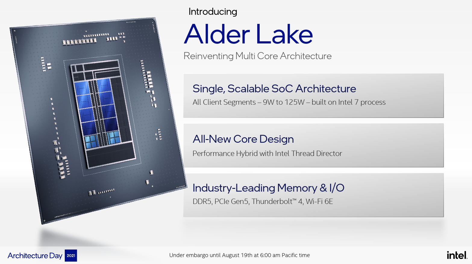
Two years ago, Intel starting experimenting with heterogeneous multi-core SoCs in commercialized products with the introduction of Lakefield. Lakefield largely served as a proof-of-concept for the company. At the time, it was still missing a few things to make it a more viable product in the mainstream client market. This year, at Intel’s 2021 Architecture Day, the company unveiled Alder Lake – their next-generation mainstream client SoC which will be the company’s first mass-market mainstream heterogeneous multi-core SoC.
This article is part of a series of articles covering Intel’s 2021 Architecture Day:
- Intel’s Gracemont Small Core Eclipses Last-Gen Big Core Performance
- Intel Details Golden Cove For Next-Generation Client and Server CPUs
- Intel Unveils Alder Lake: Next-Generation Mainstream Heterogeneous Multi-Core SoC
- Intel Unveils Sapphire Rapids: Next-Generation Server CPUs
- Intel Introduces Thread Director For Heterogeneous Multi-Core Workload Scheduling
- Intel’s Mount Evans: Intel’s First ASIC DPU
- Intel Unveils Xe HPG – Discrete Graphics For Gamers
- Intel Unveils Xe HPC And Ponte Vecchio
Gracemont + Golden Cove
Alder Lake is Intel’s next-generation client SoC and the successor to Tiger Lake. Fabricated on Intel 7 process, Alder Lake is designed to scale from the ultra-mobile 9 W market all the way to the 125 W desktop market. Unlike prior generations, Alder Lake will be the first mainstream client heterogeneous multi-core – featuring up to 8 big Golden Cove cores along with up to 8 small Graceomnt cores. But assigning threads to the proper cores is a complex task. Intel Lakefield struggled with that. Since the launch of Lakefield, Intel has been working on a technology they call Thread Director which provides the operating system with the hardware performance telemetry, allowing the operating system to do real-time contextual thread migration based on the executing instruction stream.
One of the things worth talking about is ISA support. While Golden Cove supports AVX-512 along with new extensions, the efficient Gracemont core only supports up to AVX2. In order to resolve the mismatch in the ISA level of support, on Alder Lake, the Golden Cove core has the entire AVX-512 ISA entirely fused off.
Different Configuration For Different Markets
While the base architecture is the same, Alder Lake is offered in slightly different configurations depending on the market segment. There are three major configurations for three key segments of the client market. For the desktop market, the highest performance chips will be offered in a new LGA-1700 package. In the mobile segment, a much smaller form factor is offered in a BGA Type3 package. This chip will also offer Intel’s image signal processor, larger integrated graphics, and Thunderbolt 4 connectivity. For the ultra-mobile segment, a much denser BGA Type4 HDI package is used with optimized I/O.
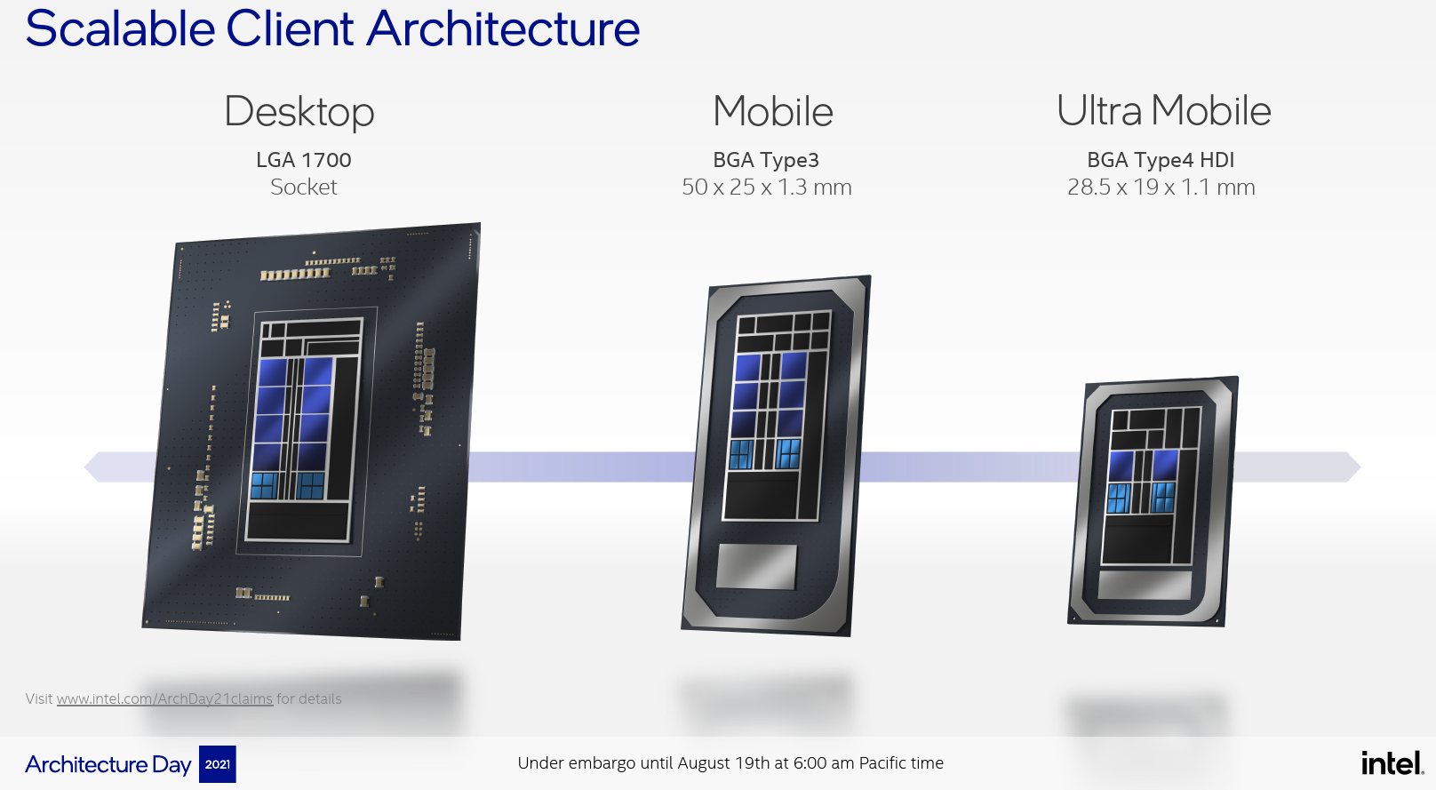
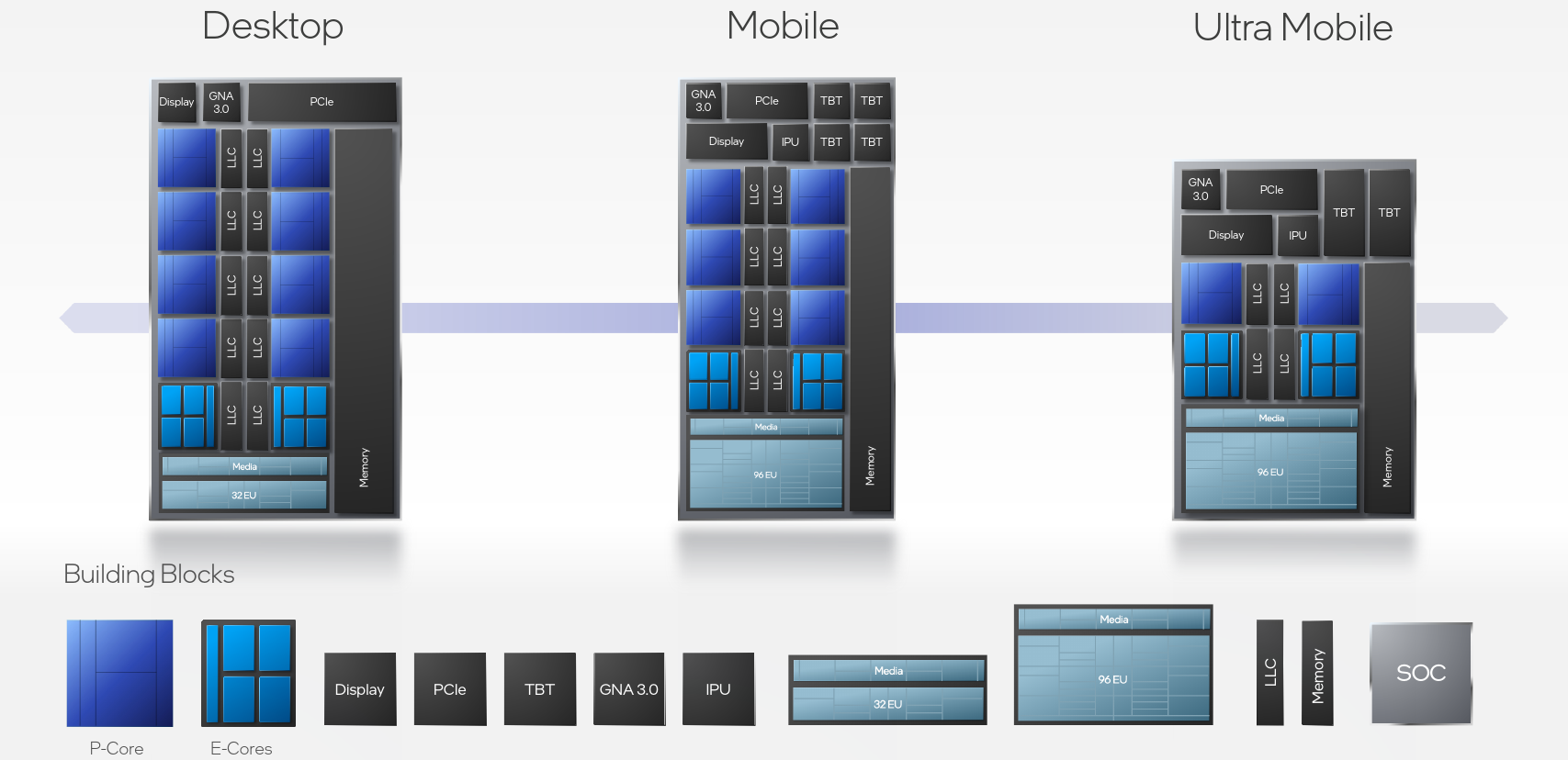
For Alder Lake, Intel designed an array of components that may be combined as desired to form targetted market configuration. Intel’s big performance cores (also called P-Cores) and Intel’s small efficiency cores (also called E-Cores) can be integrated interchangeably on the Alder Lake SoC fabric. The various I/O PHYs and other accelerator blocks such as the IPU and GNA can also be added as needed along with the various integrated GPU configurations.
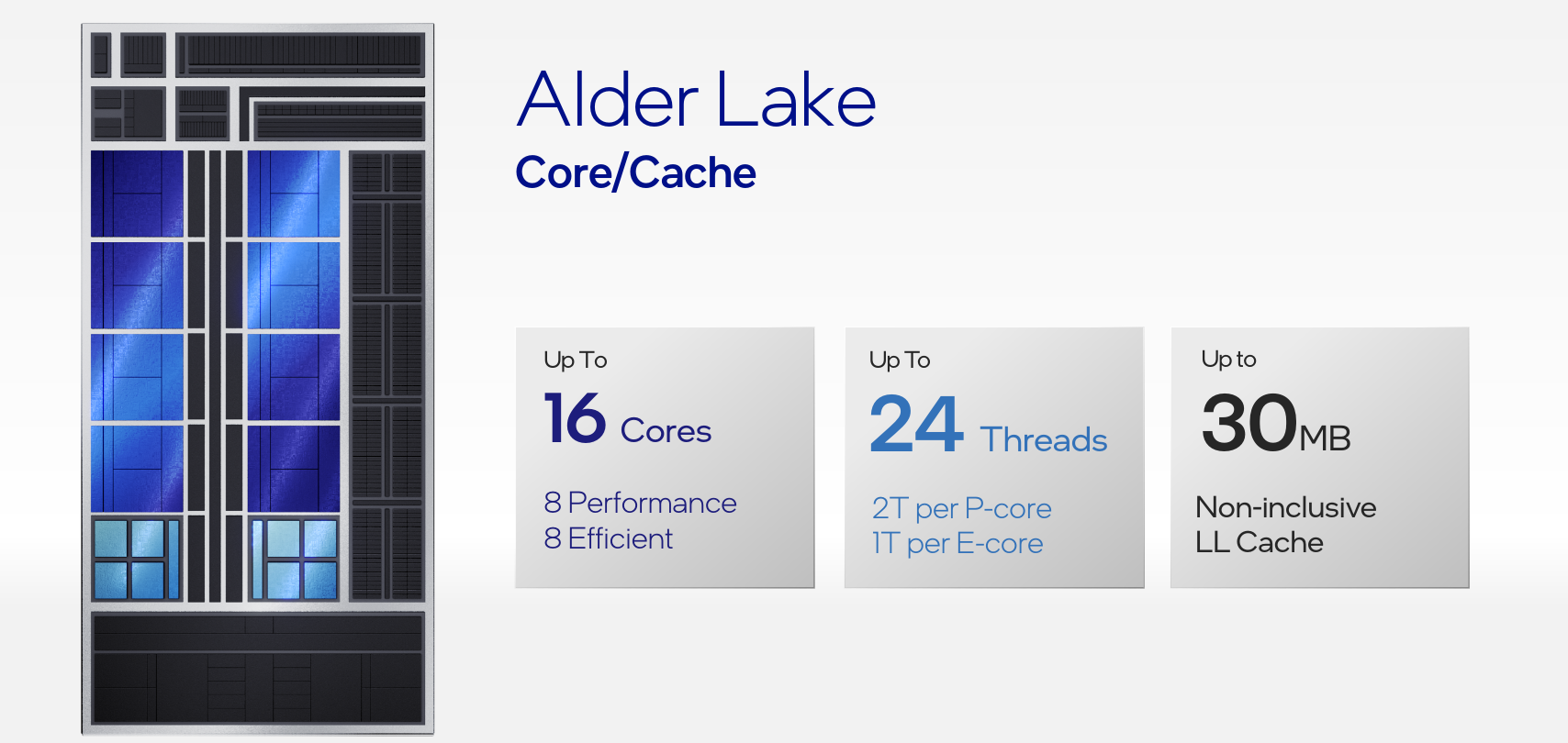
To that end, Alder Lake integrated up to eight P-Cores and up to eight E-Cores. Because the eight Golden cove cores each support multi-threading, a maximum Alder Lake configuration may have up to 24 threads in total. In that configuration, the last level cache can have a capacity of up to 30 MiB.
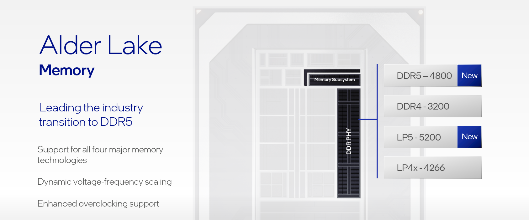
Memory
Alder Lake is introducing support for both DDR5 and LPDDR5 with data rates of up to 4800 MT/s and 5200 MT/s respectively. The actual bandwidths vary in real-time by the SoC based on the workload heuristics being executed in order to lower power consumption when possible. One unique aspect of the new memory controller is that it’s a new unified memory controller, supporting both the new DDR5/LPDDR5 specs along with the prior DDR4 and LPDDR4x specifications – all in a single chip. This means that cost-sensitive devices may still be able to utilize DDR4 while allowing high-end devices to take advantage of the new memory modules.
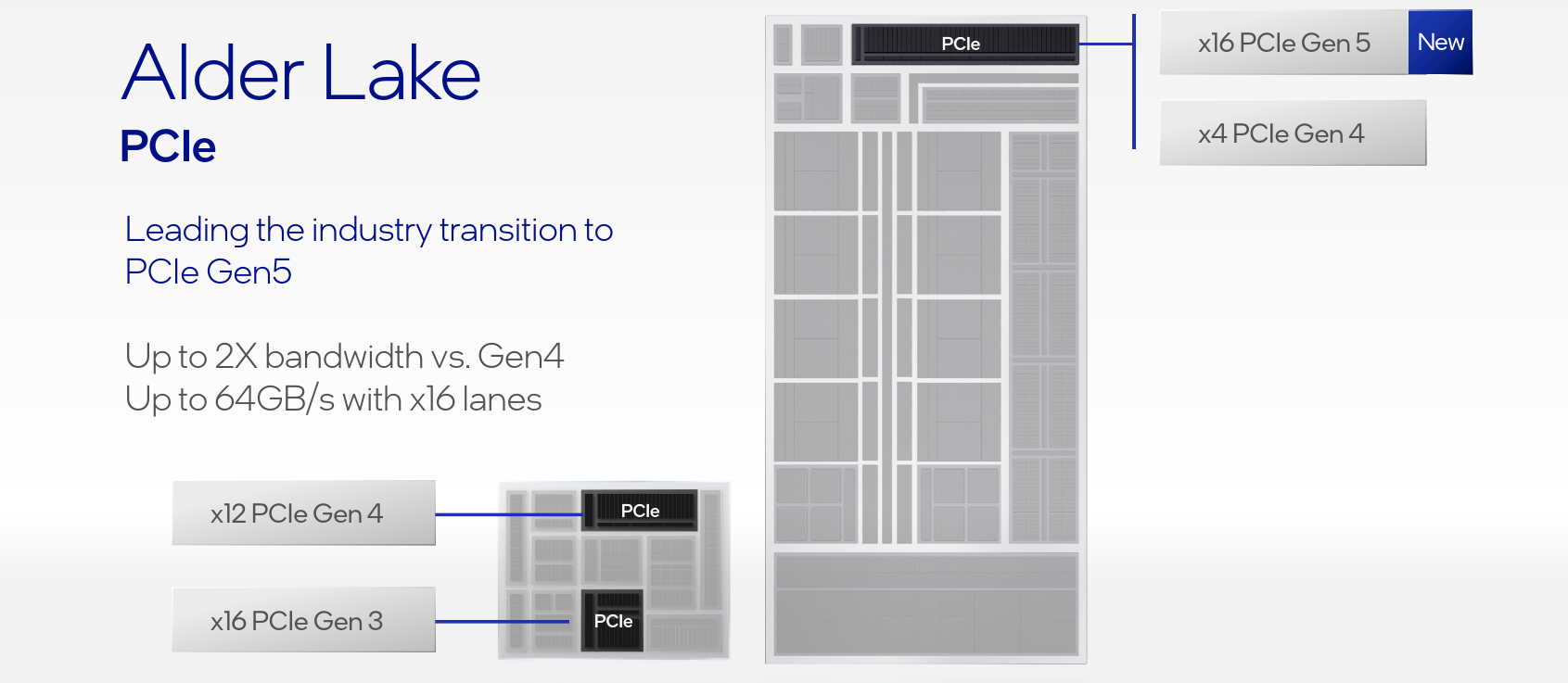
I/O
As with the memory subsystem, Alder Lake received a series upgrade on the I/O side. The new SoC now supports PCIe Gen5 which offers twice the effective bandwidth of Gen4 – at 64 GB/s of bandwidth. Alder Lake supports x16 lanes of PCIe Gen 5 along with x4 of PCIe Gen 4 lanes on the desktop parts. For the mobile segment, the SoC supports up to x12 lanes of PCIe Gen4 along with up to x16 lanes of PCIe Gen3.
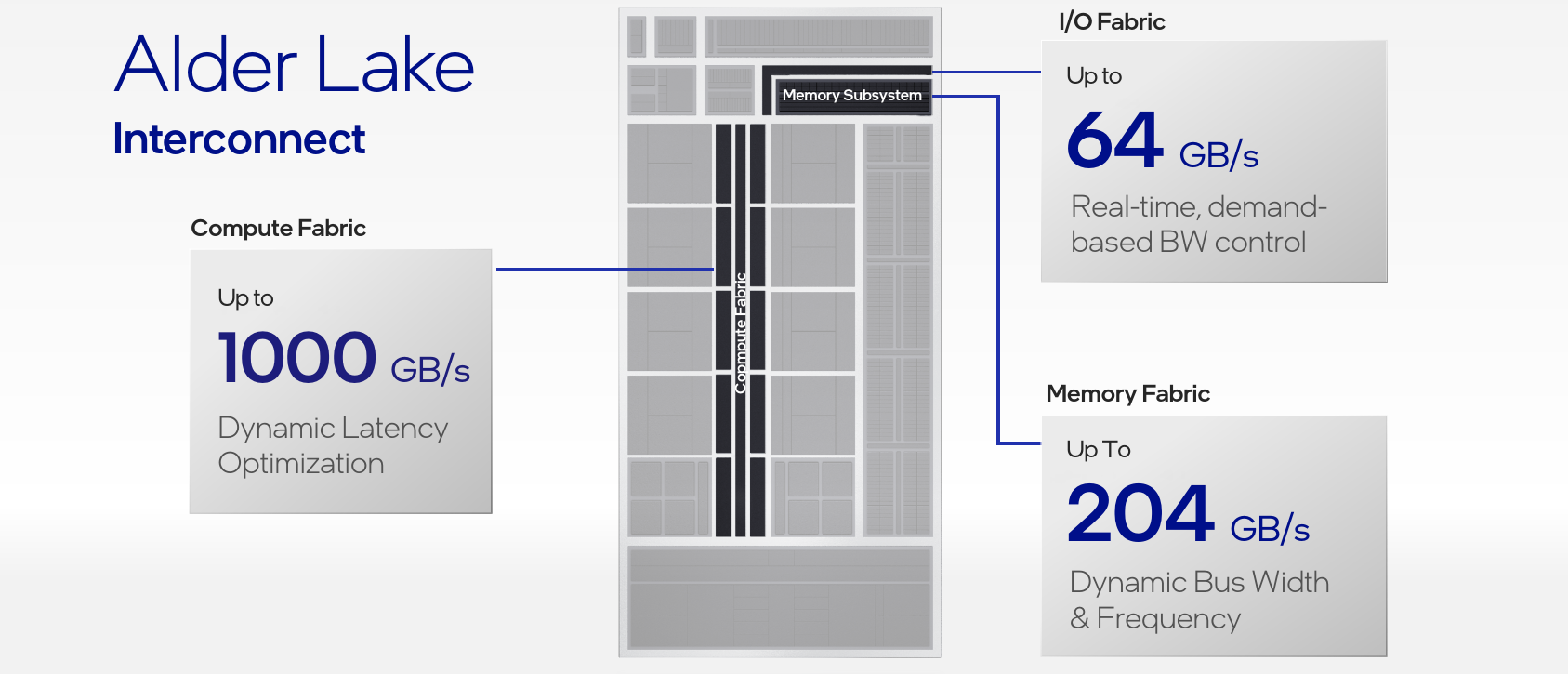
Interconnect
Alder Lake features a number of fabrics that join the various class of components together. The P-Cores and E-Cores are interconnected via the company’s ring interconnect which on Alder Lake supports total bandwidth of up to 1,000 GB/s. With a total of 10 cores (P-Cores)/clusters (E-Cores), this works out to roughly 100 GB/s per core. The ring interconnect connects all the cores and core clusters together as well as to the integrated graphics and the system uncore. The ring interconnect on Alder Lake is said to have a high dynamic frequency range and depending on the workload, it is capable of dynamically adjusting the path for either bandwidth or latency. Additionally, it has the ability to adjust the LLC slice behavior – for example being exclusive or inclusive based on utilization.
All the I/O controllers and internal devices and accelerators are interconnected via the I/O fabric. Like the compute fabric, the I/O fabric can also adjust its speed to optimize performance versus power depending on the workload. The I/O fabric is capable of up to 64 GB/s of bandwidth.
This article is part of a series of articles covering Intel’s 2021 Architecture Day:
- Intel’s Gracemont Small Core Eclipses Last-Gen Big Core Performance
- Intel Details Golden Cove For Next-Generation Client and Server CPUs
- Intel Unveils Alder Lake: Next-Generation Mainstream Heterogeneous Multi-Core SoC
- Intel Unveils Sapphire Rapids: Next-Generation Server CPUs
- Intel Introduces Thread Director For Heterogeneous Multi-Core Workload Scheduling
- Intel’s Mount Evans: Intel’s First ASIC DPU
- Intel Unveils Xe HPG – Discrete Graphics For Gamers
- Intel Unveils Xe HPC And Ponte Vecchio
–
Spotted an error? Help us fix it! Simply select the problematic text and press Ctrl+Enter to notify us.
–