
A look at Nvidia’s NVLink interconnect and the NVSwitch
A little over a month ago at their annual GPU Technology Conference (GTC) 2018, Jensen Huang, Nvidia’s CEO, announced the DGX-2. The $399K, 350-pound machine designed specifically to accelerate AI workloads, was dubbed “the world’s largest GPU.” To see why it’s such a fitting name and how we got here, we have to go back a couple of years.
Motivation
Prior to Nvidia’s current solution, in order to form more powerful compute nodes, multiple GPUs were connected over a PCIe switch and directly to the CPU.
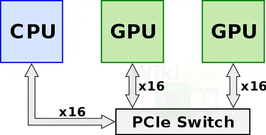
With close to 32 GB/s bidirectional bandwidth for x16 PCIe Gen 3.0, as the training data sets grew, the interconnects themselves became a critical system bottleneck. Without improving the interconnect bandwidth, the added performance offered by new generations of GPUs would not materialize in real-world workloads.
NVLink
To address this problem Nvidia developed a new interconnect architecture called NVLink. A single NVLink is a bidirectional interface incorporating 32 wires forming 8 differential pairs in each direction. The first implementation of this, NVLink 1.0, was introduced with the P100 GPU. The P100 incorporated four NVLinks. With 40 GB/s bidirectional bandwidth per link, the chip had an aggregated bandwidth of 160 GB/s.
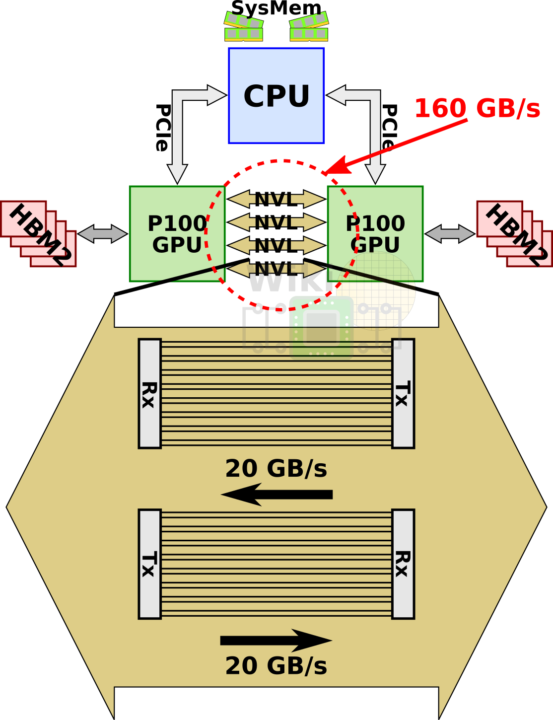
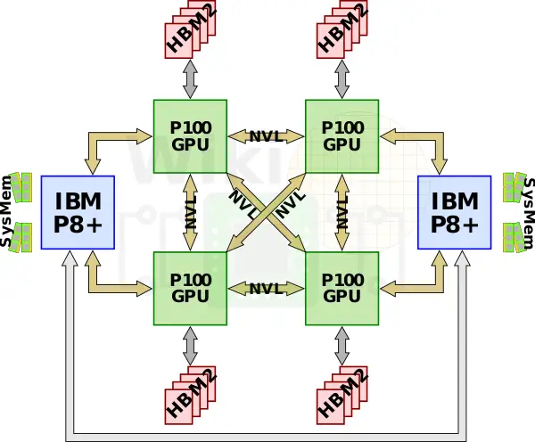
NVLink isn’t exclusively a GPU-GPU interconnect. IBM added NVLink 1.0 support to their POWER processors with the POWER8+ microarchitecture. This allows the P100 GPUs to communicate directly with the CPU over an NVLink instead of PCIe. A 4-GPU node can be configured in a fully-connected mesh as well as to the nearest POWER8+ CPU.
DGX-1
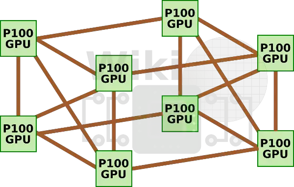
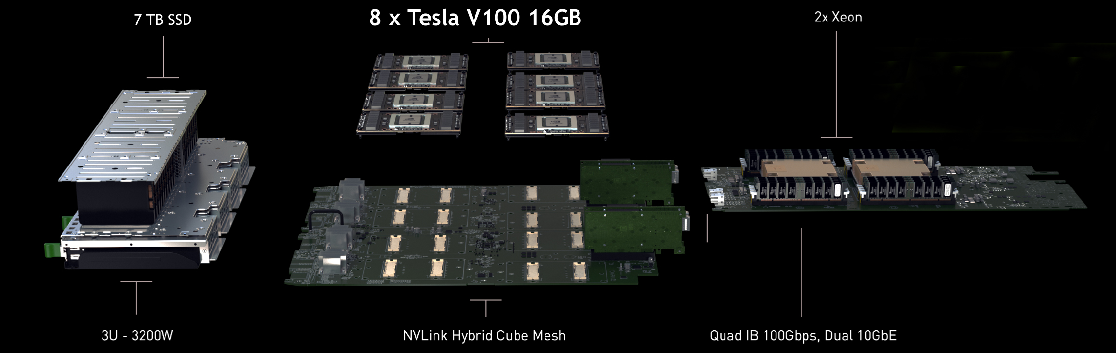
The first special-built machine by Nvidia for AI acceleration was the DGX-1 which incorporated eight P100 GPUs along with dual-socket 20-core Xeon E5-2698 v4. Since each GPU only has four NVLinks, the GPUs are connected in a hybrid cube-mesh network topology whereby a group of four fully-connected GPUs is connected to the second group of fully-connected GPUs.
Since the GPUs need more PCIe lanes than supported, each pair of GPUs is connected to a PCIe switch. The two Xeons operate as a two-way multiprocessor connected over Intel’s own QPI links.
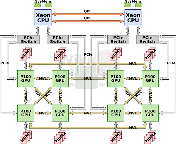
With eight Tesla P100 GPUs and 16 GiB of memory per GPU, the machine had 128 GiB of GPU memory and an additional 512 GiB of DDR4-2133 system memory.
NVLink 2.0
Nvidia introduced second-generation NVLink 2.0 with the GV100. Support from IBM came with the recently launched POWER9 CPUs. NVLink 2.0 increased the signaling rate from 20 Gb/s to 25 Gb/s for a bidirectional bandwidth of 50 GB/s per link. The V100 also increased the number of NVLinks implemented on-die to six. This bumps the aggragated bandwidh of the V100 from 160 GB/s in the P100 to 300 GB/s.
By the way, in addition to the bandwidth improvement, Nvidia added a number of new operational features to the protocol itself. One of the more interesting features they added is the introduction of coherency operations, allowing the CPU caches to store GPU memory on data reads, significantly reducing latency accesses.
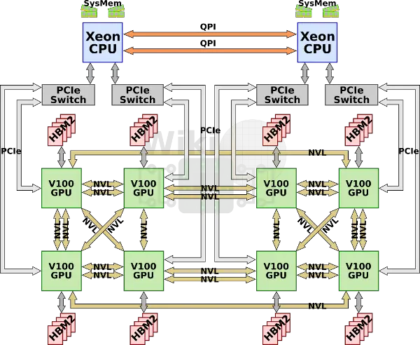
Last year, Nvidia upgraded the original DGX-1 to V100s. Since the overall topology did not change, the extra links were used to double up some of the existing inter-GPU links.
DGX-2
Announced at GTC 2018, the DGX-2 doubles the amount of V100 GPUs to sixteen. Interestingly, Nvidia also upgraded the HBM2 memory installed to 32 GiB for a total of 512 GiB of HBM2 memory. The CPUs have also been upgraded to dual-socket 2.7 GHz 24-core Xeon Platinum 8168.
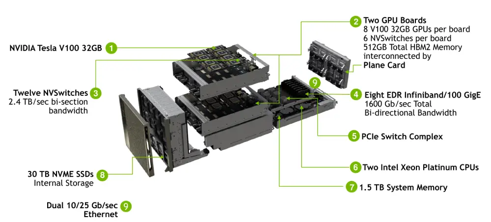
Scaling the machine to sixteen GPUs requires significant changes to the system, particularly as far as network bandwidth is concerned.
NVSwitch
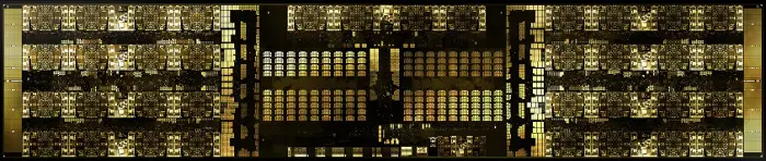
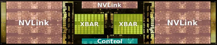
With the DGX-2, Nvidia introduced a new ASIC – the NVSwitch. The NVSwitch is a dedicated NVLink switch with 18 NVLink ports implemented. The chip itself has been under development for over two years. By supporting NVLink 2.0 this means each port has a bidirectional bandwidth of 50 GB/s for an aggregated bandwidth of 900 GB/s. The chip itself is 100 W fabricated on TSMC’s 12nm FinFet (12FFN, an enhanced 16nm node for Nvidia) with 2 billion transistors.
The chip is packaged in a 1,940-pin 4 cm² BGA package. With 18 NVLinks, 576 of those pins are dedicated to NVLink signals with the remaining used for the power rails as well as some of the other I/O which include x4 PCIe Gen 2 management port, I²C, and GPIO.
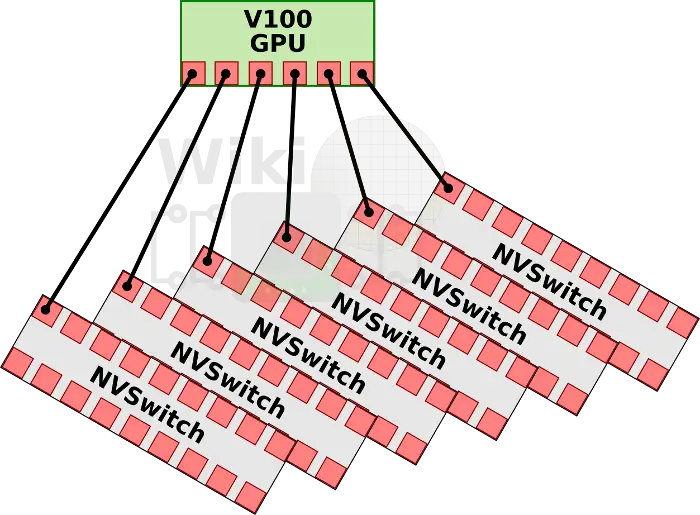
With 18 ports, the NVSwitch allows NVidia to design a fully non-blocking fully-connected 16-GPU system. With 6 NVLinks per V100, each link is connected to a separate NVSwitch.
This is repeated for all eight of the V100 GPUs for a total six NVSwitches. The final design is a single baseboard featuring eight fully connected GPUs using six NVSwitches.
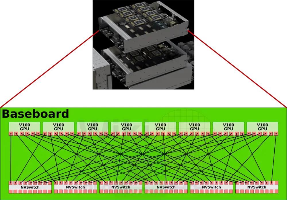
The DGX-2 has two baseboards fully linked together using the NVSwitches on each of the baseboards forming a system of 16 fully-connected GPUs.
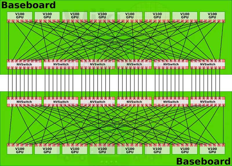
Note that there are eight links going between each of the NVSwitches correspondings to the eight GPUs on each of the baseboards. With 6 NVLinks per V100 and 16 GPUs in the DGX-2, this works out to 2,400 GB/s of total bisectional bandwidth. What’s interesting is that the NVSwitches have 18 ports, but the DGX-2 only makes use of 16 of them. It’s possible Nvidia has left the other two links to support IBM’s POWER9 (note that both the DGX-1 and 2 have been using Intel’s Xeons). In this hypothetical topology, a single IBM POWER9 processor can be connected to each of the baseboards meaning all the GPUs will also be fully-connected to the POWER9 processors. By having the CPUs directly connected to the NVSWitches, the PCIe switch tree that is required to connect the GPUs to the current Intel processors could be eliminated. Nvidia has not disclosed any plans for selling the NVSwitches directly to manufacturers, but if they do, it would allow for different and possibly larger (albeit not necessarily fully connected) compute nodes.
In the original DGX-1, transactions between some GPUs required one additional hop making remote accesses inconsistent. This made exploiting unified memory rather problematic for many workloads. With the DGX-2, since every GPU can now talk to every other GPU at the same speed and consistent latency, large AI workloads can take advantage of model parallelism techniques. Back at GTC Nvidia dubbed the system the “the world’s largest GPU.” In practice, since every GPU is now linked to every other GPU, unified memory has been simplified. It’s now possible to virtually combine the 512 GiB of high-bandwidth memory and treat it as a single unified memory. Both the GPU and the NVSwitch implement algorithms to aid the memory subsystem. As far as the program is concerned the entire machine can be treated as a single large GPU with the memory subsystem taking care of the memory layout to provide an optimal organization.
Derived WikiChip Articles: NVLink.
–
Spotted an error? Help us fix it! Simply select the problematic text and press Ctrl+Enter to notify us.
–