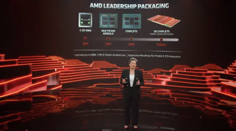
A Look At AMD’s 3D-Stacked V-Cache
[Subscription] A technical look at AMD’s 3D-Stacked V-Cache
Read more
Your Chips and Semi News
[Subscription] A technical look at AMD’s 3D-Stacked V-Cache
Read more
Samsung tapes out 3nm GAA test vehicle as it inches towards mass production
Read more
IBM doubles its 14-nanometer eDRAM density through physical design work, enabling the packing of hundreds of additional megabytes of cache on the latest z15 microprocessor and system controller.
Read more
CEA-Leti demonstrates a high-performance microprocessor architecture with a 96-core MIPS processor built with six chiplets 3D-stacked on an active interposer die.
Read more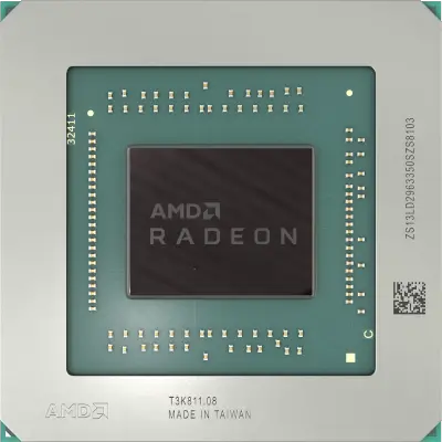
A look at AMD’s Radeon RX 5700 GPU built on a 7-nanometer process based on the new Navi microarchitecture and RDNA graphics architecture.
Read more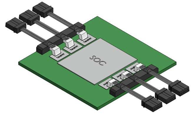
Integrated photonics has long been considered a holy grail for communication. Ayar Labs TeraPHY chiplet represents a major step forward through the co-packaging of the optical interface along with an SoC.
Read more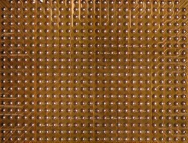
A look at the 496-core RISC-V manycore array, network-on-chip, and the digital PLL of the Celerity open-source RISC-V tiered accelerator.
Read more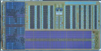
From a DARPA vision and a $15 million seed to a commercialized CMOS silicon photonics product: how Ayar Labs collaboration with GF produces a photonics chiplet that can supercharge Intel FPGAs.
Read more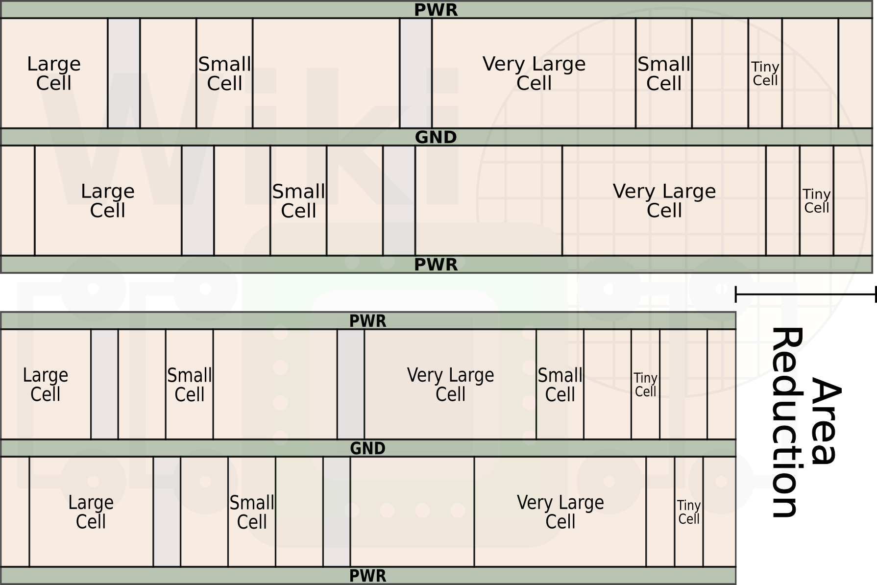
Presented at the 64th IEEE International Electron Devices Meeting (IEDM) in December, here’s a look at Intel’s 10-nanometer standard cell library and power delivery system.
Read more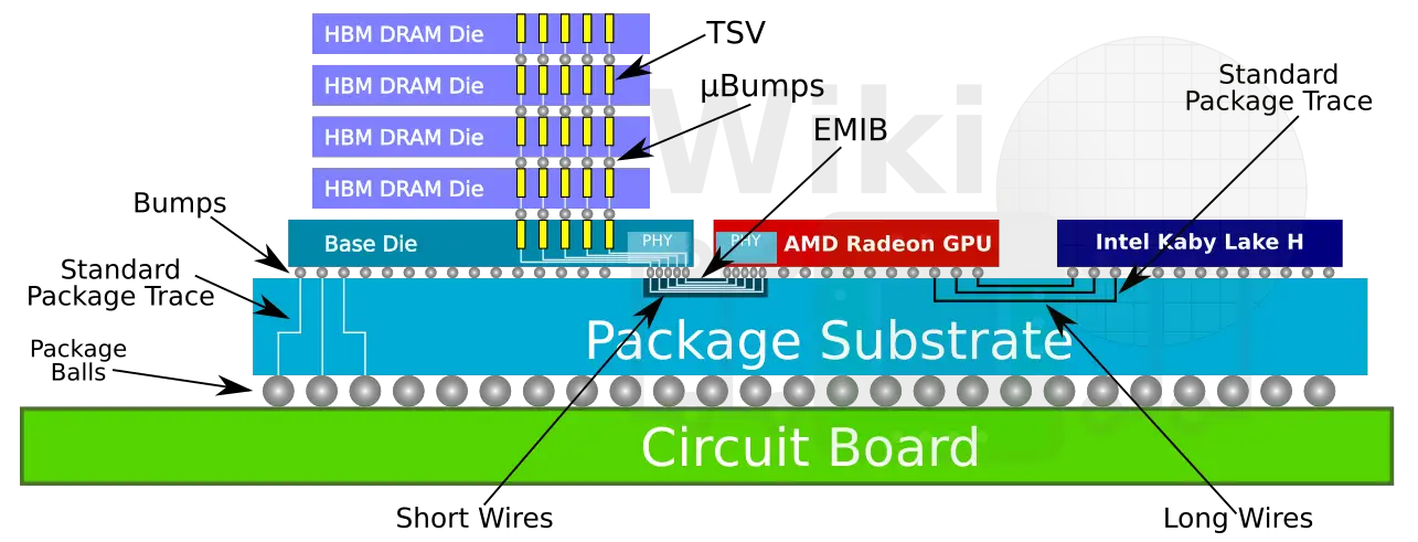
A look at Intel’s current generation of Thin & Light processors with high-performance graphics, formerly known as Kaby Lake G, from Hot Chips 30.
Read more