
Ayar Labs Realizes Co-Packaged Silicon Photonics
High-performance computing demand high-performance I/O. The industry has been struggling with improving high-bandwidth long-range solutions for some time. Last year saw the introduction of FPGAs from both Intel and Xilinx with 56G I/O. Long-reach 112G SerDes PHYs have been announced and will likely be in better shape with the upcoming 5-nanometer node. Looking a bit further out, industry roadmaps beyond 112G is filled with uncertainties. For longer distances that span dozens of meters or more, optical communication is used instead of electrical. Unfortunately, those products tend to be inversely related. The further from the physical die you get, the costlier it is to transmit a bit. Likewise higher wire data rates typically sacrifice density. It’s for this reason that monolithic silicon photonics is seen as the holy grail solution for information processing.
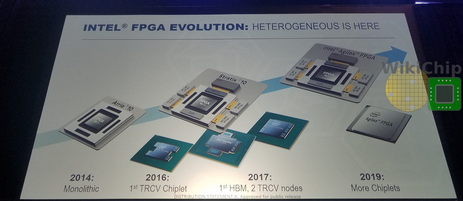
The last decade saw the significant commercial introduction of numerous ways of enabling higher integration. Silicon interposers such as TSMC CoWoS and Samsung I-Cube as well as silicon bridges such as Intel’s EMIB have allowed for high-volume production of chips that integrate multiple dies tightly on the same package. First products to market enabled high-bandwidth DRAM by moving the DRAM dies right next to the compute die, improving the bandwidth and reducing the power. Beyond memory, there is a large effort to enable support for combining multiple niche-purpose dies – more appropriately termed chiplets in this case – together on a package in order to enhance the capabilities of the chip. Although today, most chiplet-based designs involve only own-developed chiplets, future designs will likely combine dies from multiple companies. The oldest such effort is from Intel for its Stratix 10 FPGA family which consists of a monolithic FPGA die that incorporates multiple AIB links. These links allowed Intel to offer many different SKUs with varying chiplets (called tiles for their product) options such as HBM tiles, Transceiver tiles, UPI tiles, and even 3rd-party designs. More recently, the OCP has announced it formed its own working group to drive industry-wide chiplets standards.
![]()
Ayar Labs is a silicon photonics startup based in Emeryville, California. The company raised $24 million in Series A Funding. Ayar is taking the unusual approach of going after the processor market instead of networking. Their premise is quite simple – move optics as close as possible to the compute die in order to achieve better bandwidth and energy efficiency. In other words, realize near-monolithic photonics integration in order to enjoy the best of both worlds – get the per bit transfer energy efficiency that is comparable to other in-package components while enabling long-range communication that can span dozens to hundreds of meters.
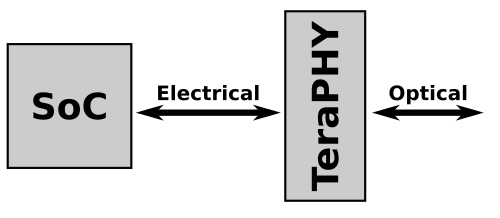
Enter TeraPHY
The Terabit PHY, or TeraPHY for short, is Ayar Lab’s first product. This is a prototype photonics chiplet that is designed to be integrated into a package along with a CPU, GPU, or an FPGA in a system-in-a-package. There is just one small catch – optics and electrical don’t exactly talk to each other. The secret? Ayar’s design leverages GlobalFoundries 45nm RF SOI (Radio Frequency Silicon on Insulator) process which allows them to develop monolithic designs that integrate both the optical components and a complex set of electric circuits around those optical devices on a single piece of silicon. Simply put: this allows them to expose an electrical I/O interface on one side and an optical interface on the other side.
Last year WikiChip reported on the Ayar Labs and GlobalFoundries collaboration with Intel. Intel has already developed an extensive chiplet architecture around its Stratix 10 FPGA family. But all those chiplets were developed in-house. The good news is that the architecture uses the AIB interface to communicate between the main FPGA die and the various chiplets. The interface was also opened up as an open standard as part of the DARPA ERI effort so it’s no longer exclusive to Intel or EMIB. The Stratix 10 multi-chip architecture lends itself to the kind of functionality the TeraPHY is offering – swap out one of the electrical transceiver tiles for a TeraPHY chiplet and as long as the interfaces are compatible, you’re good to go. This is the route Ayar Labs settled on.
Electrical I/F
For TeraPHY, Ayar integrated 24 channels of the AIB interface. 24 channels are actually the maximum number of channels allowed per column (along with the AUX block). Each channel represents a group of signals. At the current bump pitch of 55-micron, this means twenty transmission data signals and twenty receiving data signals. This is a wide but low data rate interface that operates at up to 2 GT/s. Ayar says that for their TeraPHY chiplet, the total interface bandwidth is 960 Gbps which suggests they are using the 1 GT/s AIB Base specs instead of the 2 GT/s AIB Plus specs.
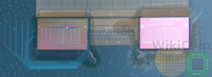
Since the AIB interface uses very small bump pitches, it’s designed to go over silicon. In the Stratix 10 case, this means using Intel’s EMIB silicon bridge technology. In the unfinished package below there are two TeraPHY chiplets on the right side of the large Stratix 10 FPGA die.
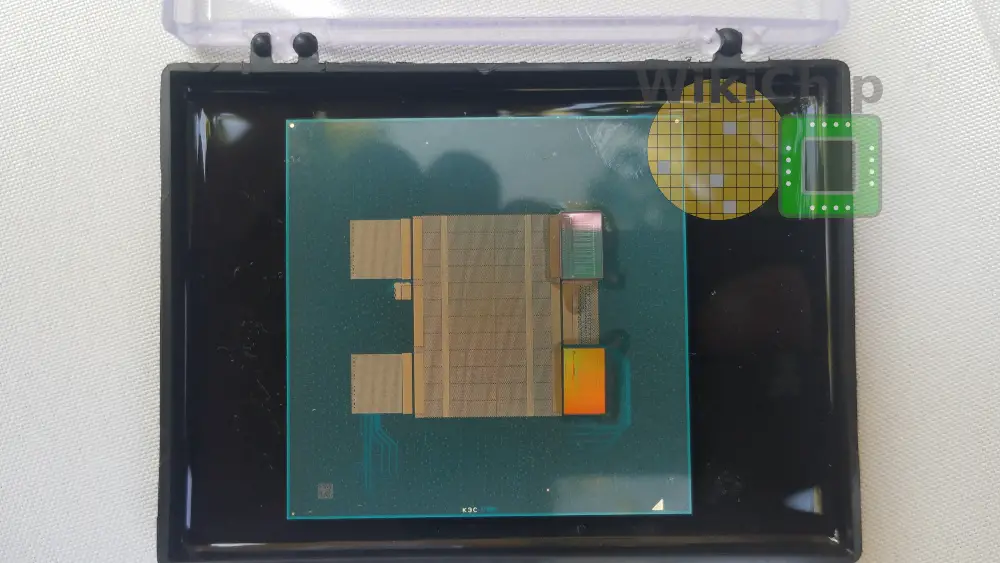
The locations of the EMIB is clearly visible at the edges of all the dies. Note that the FPGA might have additional chiplets on the other side.
–
Spotted an error? Help us fix it! Simply select the problematic text and press Ctrl+Enter to notify us.
–