
Intel Opens AIB for DARPA’s CHIPS Program as a Royalty-Free Interconnect Standard for Chiplet Architectures
The explosive growth in more specialized system-on-chip and other ASIC solutions that integrate a rich set of functional blocks has led to a sharp increase in design cost. For many research institutes and agencies such as DARPA, the cost of developing and working with leading-edge technologies with stringent requirements are becoming cost prohibitive. On the commercial side, emerging purpose-built designs for things such as artificial intelligence require integration of functions with specific performance or power requirements. For those applications, the traditional custom ASIC approach is affecting their viability from both the economic and time-to-market perspective.
DARPA’s Common Heterogeneous Integration and Intellectual Property (IP) Reuse Strategies (CHIPS) program is designed to address this problem by developing the design tools and integration standards required to develop modular electronic systems. It’s important to note that goal here is not to develop new IPs and technologies, but rather to provide a platform that would enable maximum reuse of existing IPs from many participants across various process technologies and manufacturers.
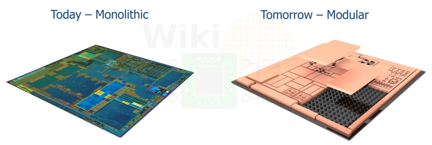
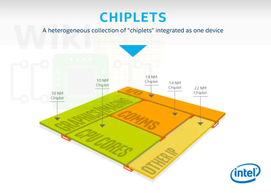
This week, DARPA is hosting the 2018 Electronic Resurgence Initiative (ERI) Summit in order to discuss future technologies, designs, and architectures. In order to take advantage of future innovations in material and process technologies, DARPA hopes CHIPS would allow keeping costs in check through increase reusability of intellectual property. Since not every IP chiplet benefits equally from what a leading-edge process has to offer, it’s becoming advantageous to manufacture those circuits on an older node while only manufacturing what’s absolutely necessary on the latest and costliest technologies. The CHIPS program does bring some pretty big fundamental changes to the design methodologies and tools that are currently being used.
To aid the CHIPS initiative, Intel is providing a royalty-free license for their Advanced Interface Bus (AIB) to CHIPS participants and others. Intel’s Advanced Interface Bus is a low-power, high-bandwidth die-to-die PHY level interface designed to allow direct chiplet-to-chiplet communication.
AIB itself is not entirely new. Intel talked a little about it before in a number of conferences. In fact, they are already leveraging AIB over EMIB with their flagship Stratix 10 FPGAs. AIB uses a forward clock parallel I/O architecture that uses single data rate (SDR) for the control signals and double data rate (DDR) for the high-speed data transfers for a rate of 2 Gbps per line. By the way, for the Stratix 10 FPGAs which use Intel’s 1st generation EMIB, they reported 1.2 pJ/b per die for a bandwidth density of 1.5 Mb/s/µm².
It’s worth noting that since this is being contributed to the DARPA CHIPS program, the Advanced Interface Bus is entirely technology agnostic; in other words, although Intel will be leveraging their EMIB packaging technologies for their own solutions, other manufacturers such as GlobalFoundries and TSMC can use it with their own solutions (e.g., CoWoS, InFO).
–
Spotted an error? Help us fix it! Simply select the problematic text and press Ctrl+Enter to notify us.
–