
Hot Chips 30: Nvidia Xavier SoC
When Nvidia left the mobile market, there was a lot of uncertainty about the future of the Tegra SoCs. Since then, Nvidia refocused their effort and the result is Xavier, an SoC designed from the ground up for controlling autonomous machines. At Hot Chips 30, Michael Ditty, Lead Architect for the Xavier SoC at Nvidia disclosed more about the chip.
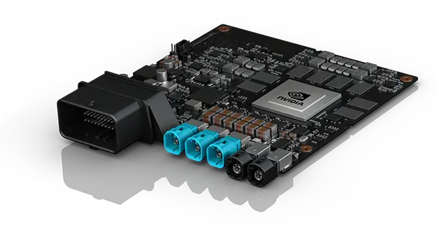
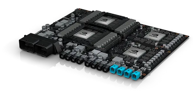
The Tegra Xavier is the successor to the Tegra Parker. Xavier can be found in a number of Nvidia products.
| Jetson Xavier | Drive Xavier | Drive Pegasus |
|---|---|---|
 |
 |
 |
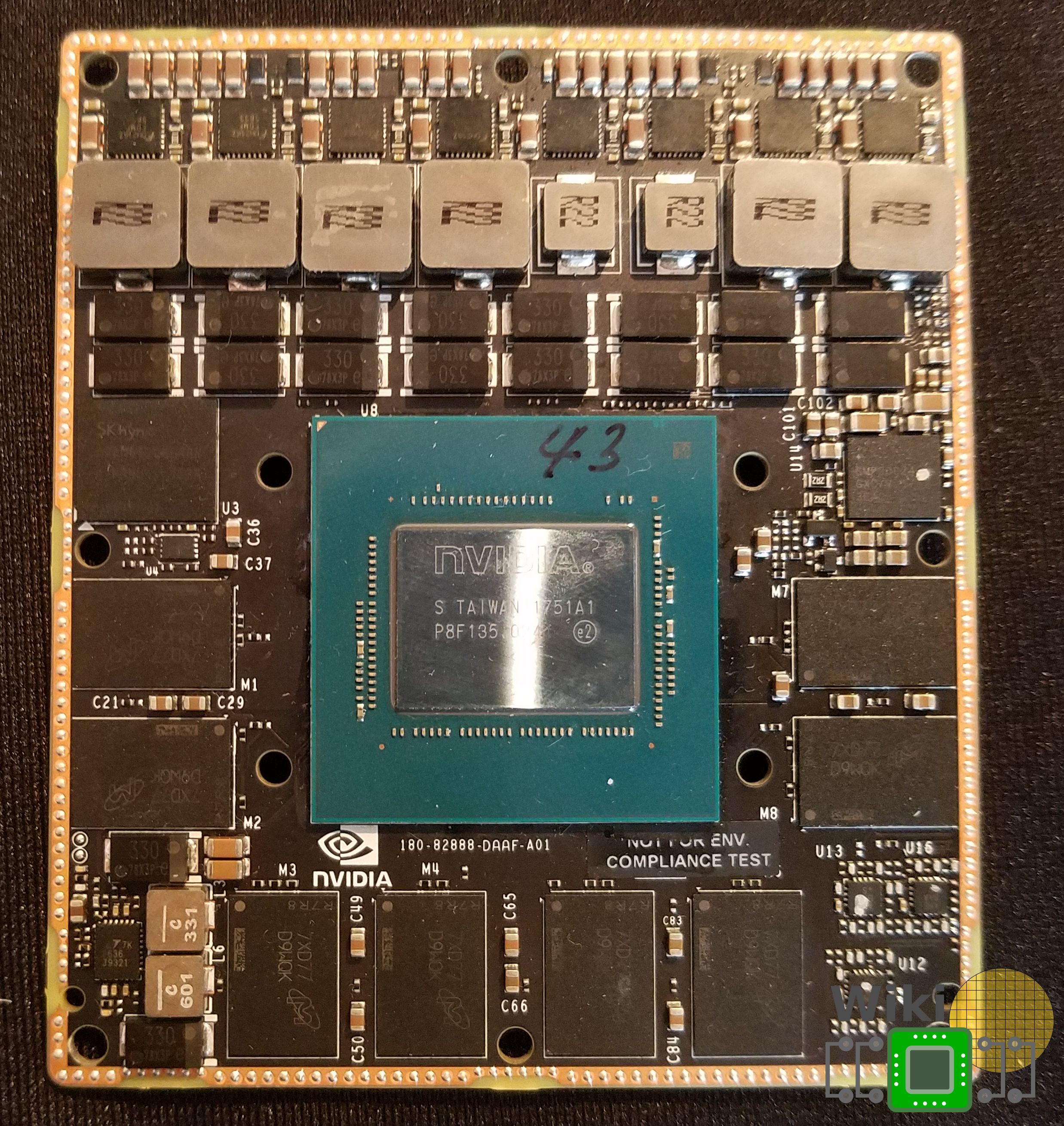
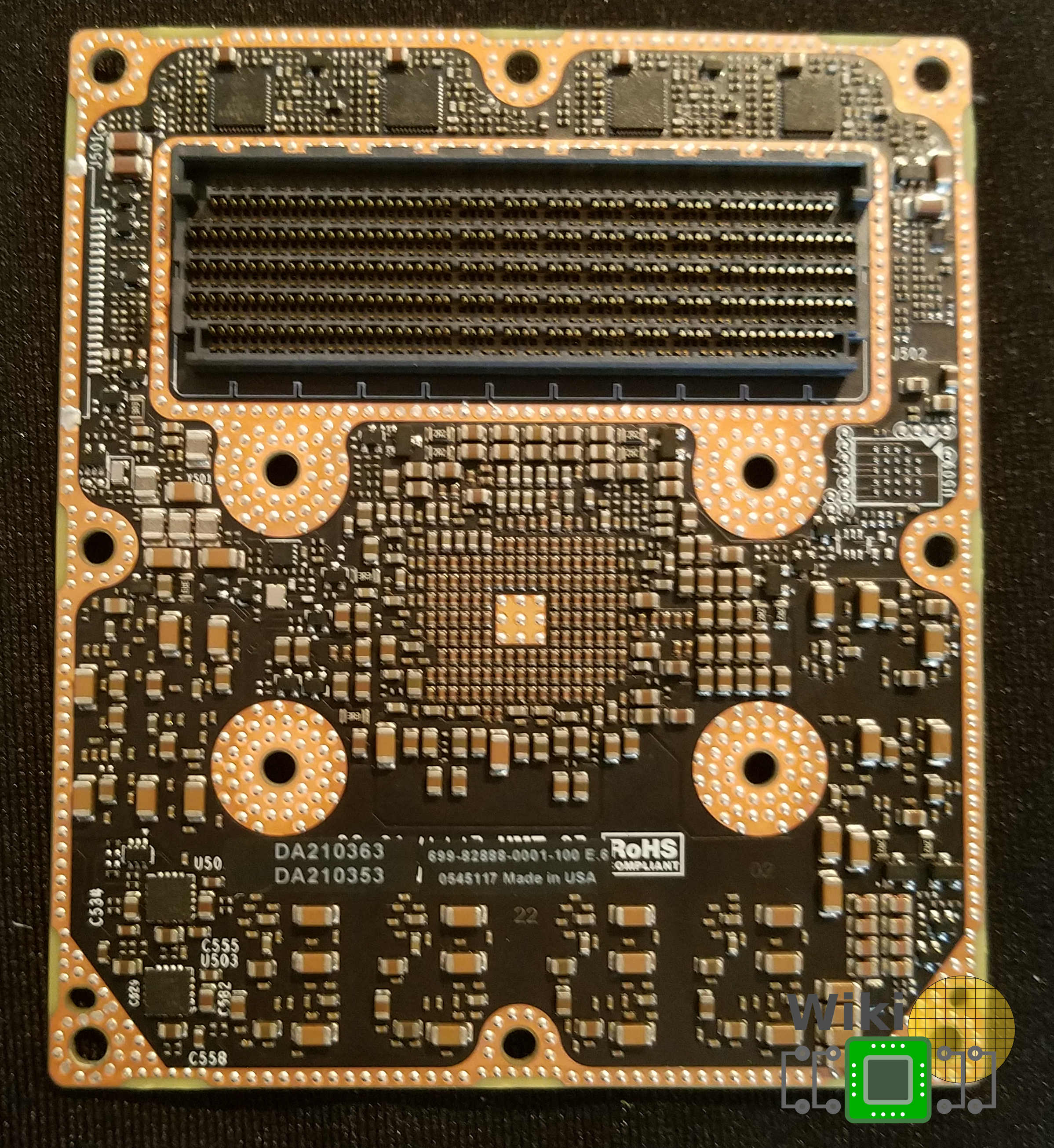
We got a few pictures of the Jetson Xavier board that was showcased at the Nvidia booth. I apologize the pictures didn’t turn out as well as we hoped.
| Front | Back |
|---|---|
 |
 |
Autonomous Machines Processor
In many ways, Xavier can be thought of as a full Tegra series reboot. The chip is designed from the ground for use in various autonomous machines ranging from autonomous cars to smart medical instruments and manufacturing equipment.
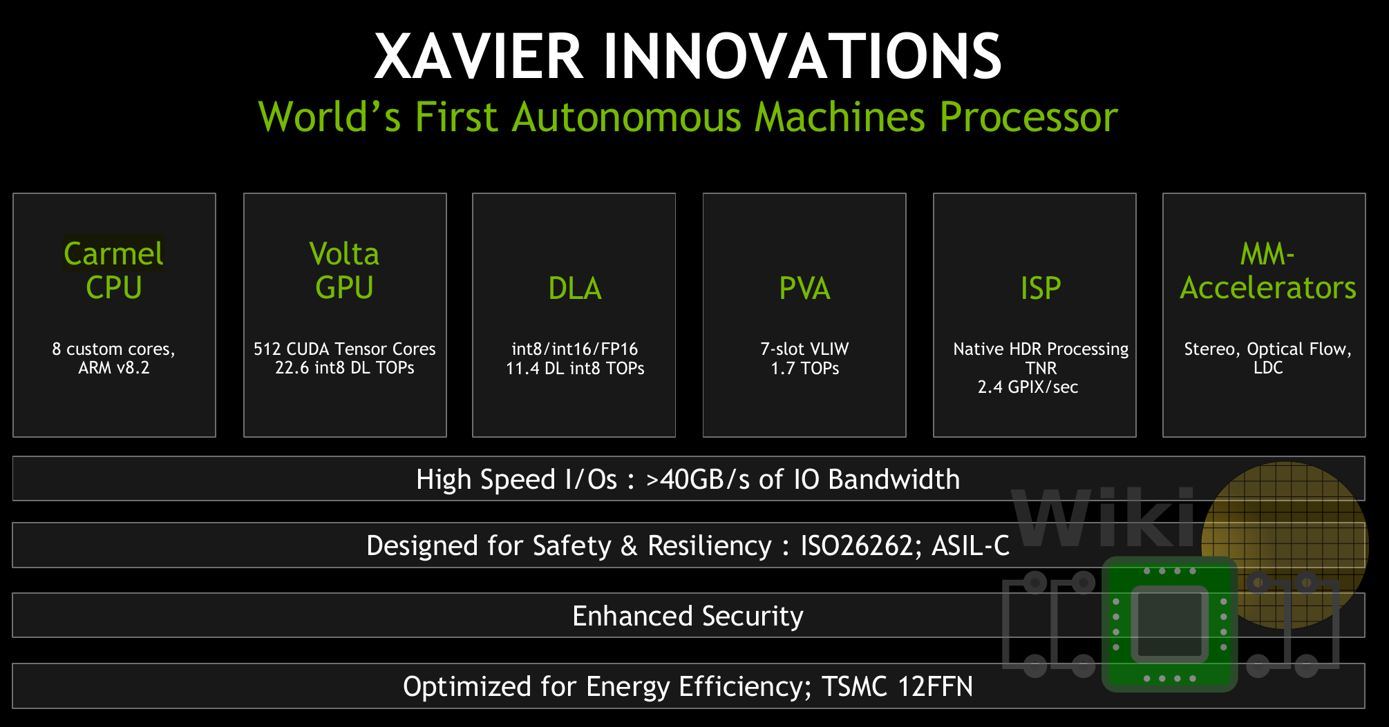
To that end, Xavier comprises a CPU, GPU, deep learning accelerator, vision accelerator, ISP, and a multimedia engine. The addition of the fixed-function accelerators might seem redundant at first but there are a quite a few classes of algorithms that can be handled more efficiently with less programmability through those that kind of logic rather than using the GPU for everything. In other words, the additional accelerators were introduced in order to augment the traditional CPU/GPU applications with a more diverse set of logic that can perform algorithms and other operations in different ways (e.g., efficiency/performance or from a safety and reliability requirement).
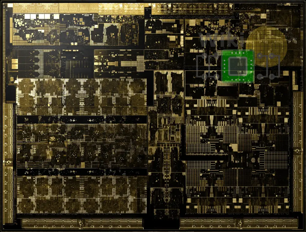
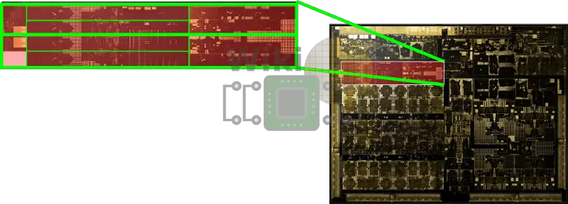
Die
Xavier consists of 9 billion transistors and is fabricated on TSMC’s 12 nm process (12FFN). The die itself measures 350 mm². What’s interesting is that when Jensen Huang first announced the Xavier SoC back in late 2016, he stated the chip has 7 billion transistors fabricated on TSMC 16FF. It’s unclear if the chip physical layout really ballooned by 1.3x or if Nvidia decided to count transistors in a slightly different way.
Volta & Carmel
Xavier implements a derivative of their Volta GPU. It has eight Volta stream multiprocessors along with a 512 KiB of shared L2. Compared to Parker, Nvidia claims this GPU has 2.1x the graphics performance. I say derivative because Nvidia made a lot of finer changes to address this specific market. Whereas their desktop parts (e.g., GV100) are a very powerful GPU that is used for training, the GPU here is optimized for inference. The most obvious change is that they added int8 support for lower precision to the CUDA tensor cores and those operate at the full 2x throughput of the FP16 ops. There is also 512 CUDA tensor cores. To put that into perspective, the GV100 has 672. All of this yields 22.6 tera-operations (int8) per second.
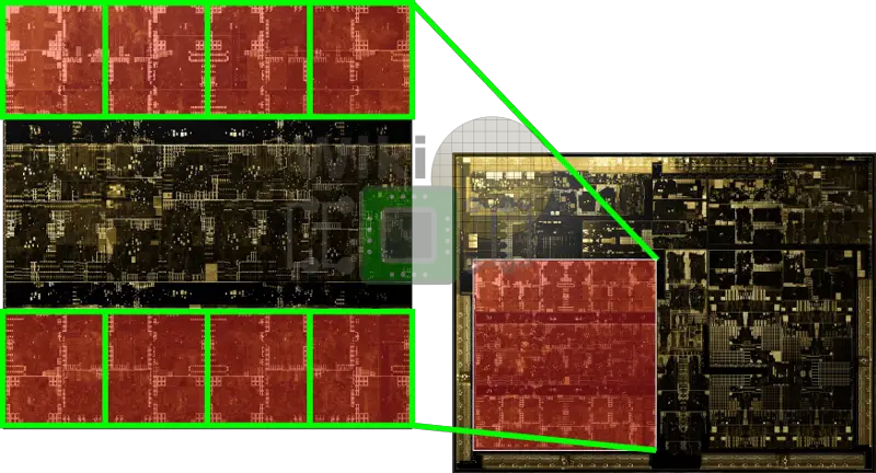
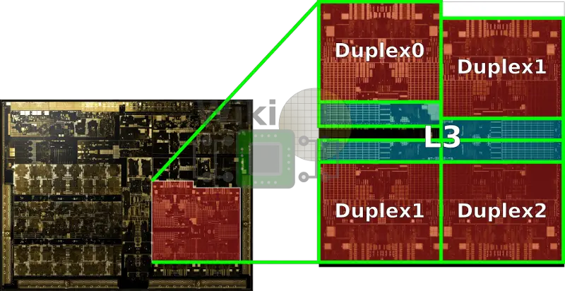
The core cluster itself was also greatly improved. The new cores are based on the Carmel microarchitecture, the successor to Denver 2, supporting ARMv8.2. The entire complex has 4 MiB of shared L3 with 2 MiB of private L2 per duplex. The primary function of the cores is to handle all the control and miscellaneous functions of the chip. It’s worth pointing out that the CPU cluster is connected to all the other accelerators through a cache-coherent fabric.
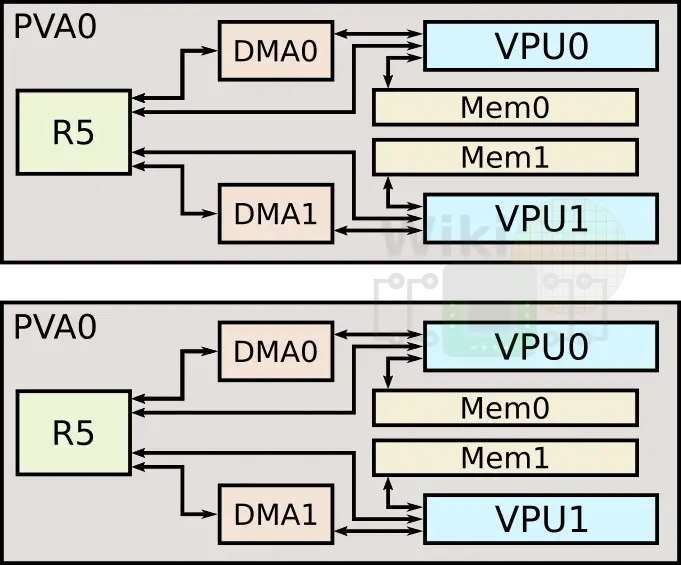
PVA
Augmenting the GPU are a set of accelerators for vision and machine learning. One of those is the programmable vision accelerator (PVA). Xavier actually incorporates two of those PVAs. Their purpose is to offer some additional design flexibility and efficiency, particularly when implementing one of the common filter loop and other detection algorithms (e.g. Harris corner).
For each of the PVAs, there are two dedicated vector processing units, each with its own memory and DMA. This 7-slot VLIW architecture made of 2 scalar slots, 2 vector slots, and 3 memory operations. The pipe is 256 bit wide and all types can operate at full throughput (32x8b, 16x16b, and 8x32b vector math).
NVDLA
One of the other accelerators on-die is the deep learning accelerator (DLA) which is actually a physical implementation of the open source Nvidia NVDLA architecture. Xavier has two instances of NVDLA which can offer a peak theoretical performance of 5.7 teraFLOPS (half precision FP) or twice the throughput at 11.4 TOPS for int8. For Xavier, Nvidia uses the large configuration which comes with both 8-bit and 16-bit support as well as extended RAM interfaces and various advanced features such as weight compression and a programmable controller which performs the sequencing based on the network without the help of the CPU, allowing the entire workload to be offloaded.
Extended WikiChip articles: Tegra Xavier, Carmel microarchitecture, NVDLA.
–
Spotted an error? Help us fix it! Simply select the problematic text and press Ctrl+Enter to notify us.
–