
Intel Cascade Lake Brings Hardware Mitigations, AI Acceleration, SCM Support
Last year Intel introduced Skylake SP, a series of microprocessors tailored for the data center. Those processors brought a large set of enhancements over Broadwell, not only at the core level, but also at the SoC level such as the introduction of mesh interconnect, an enhanced inter-chip interconnect, and support for more memory channels. The data center is becoming an increasingly important segment of Intel’s business. 2018 marked the 20th anniversary of the Xeon processor. According to Navin Shenoy, executive VP and GM of DCG, in the last 20 years, Intel has shipped over 220 million Xeon processors. Last quarter, Intel shipped over eight million units in that segment alone.

As the company continues to struggle with ramping their 10 nm process, new stopgap 14-nanometer based microarchitectures were added to their roadmap in order to maintain their yearly release cadence. Back at August, Navin disclosed their new roadmap for the next two years. Succeeding Skylake is Cascade Lake which is expected to launch next month and ramp quickly throughout 2019. The follow-up to Cascade Lake is Cooper Lake which is set to launch towards the end of 2019 with Ice Lake, a 10-nanometer design, launching sometimes in late 2020.

Cascade Lake
Expected to launch this quarter, Cascade Lake is the follow-up microarchitecture to Skylake. The architectural details of Cascade Lake were disclosed at Hot Chips 30 by Akhilesh Kumar.
Those processors are designed to be compatible with the Skylake parts (LGA-3647) and utilize the Purley platform. To that end, Cascade Lake shares the same socket and pinout as well as the same core count, cache size, and I/O.
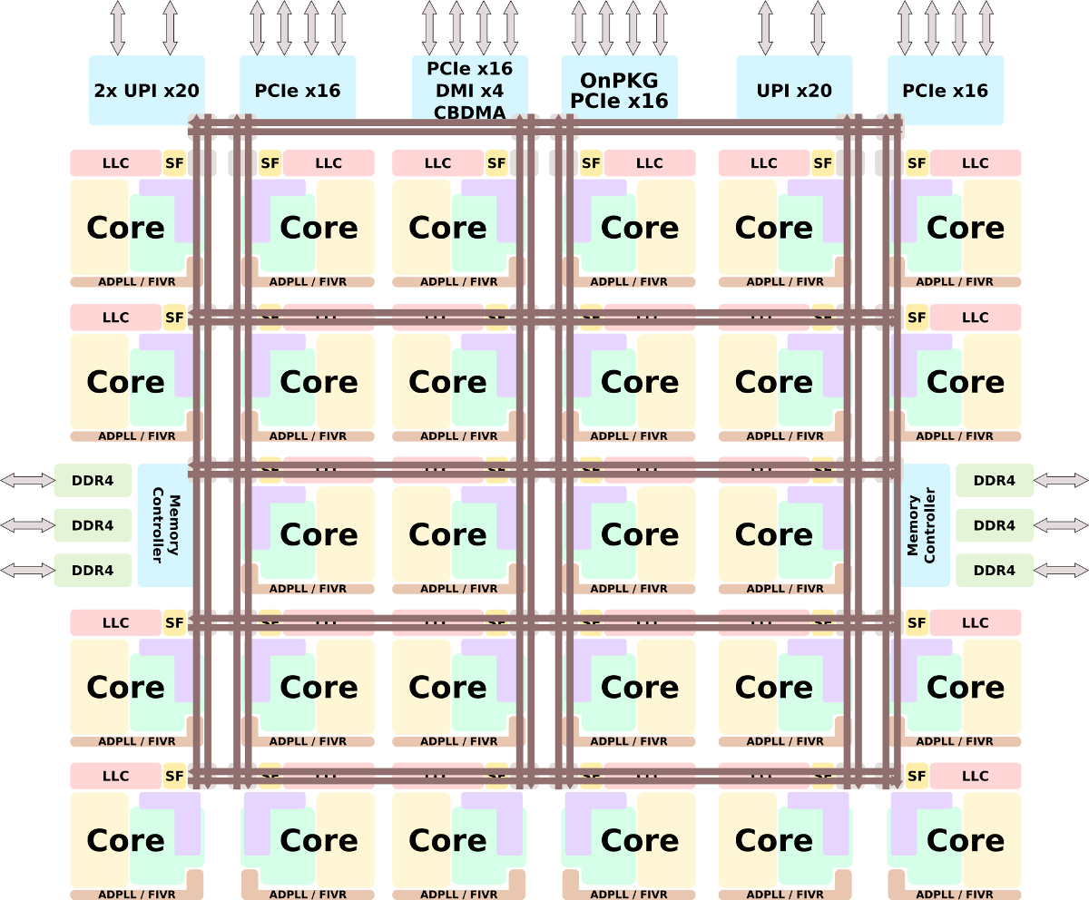
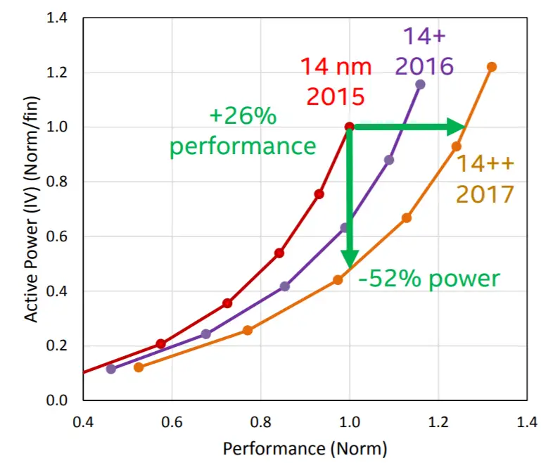
Cascade Lake is fabricated on an enhanced 14 nm process which allows Intel to extract an additional power efficiency, allowing them to clock those processors higher. Kumar also noted that targeted performance improvements were applied to some of the critical paths to make this possible.
Skylake SP was fabricated on Intel’s 14nm+ process. Intel has since introduced the 14nm++ process which brought further power and performance improvements. It’s unknown if Cascade Lake is fabricated on 14nm++ but an improved process can certainly help bring the clock speeds up by a few 100s MHz.
Side-Channel Mitigations
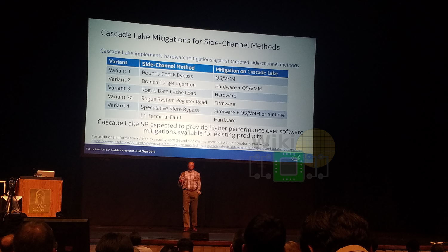
Mitigations against vulnerabilities involving side-channel analysis is a chief concern for the data center. To that end, Cascade Lake brings the first wave of silicon-based mitigations for Spectre and Meltdown.
| Cascade Lake Mitigations for Side-Channel Methods | ||
|---|---|---|
| Variant | Method | Mitigation |
| Variant 1 | Bounds Check Bypass | OS/VMM |
| Variant 2 | Branch Target Injection | Hardware+OS/VMM |
| Variant 3 | Rogue Data Cache Load | Hardware |
| Variant 3a | Rogue System Register Read | Firmware |
| Variant 4 | Speculative Store Bypass | Firmware+OS/VMM |
| L1TF | L1 Terminal Fault | Hardware |
Persistent Memory
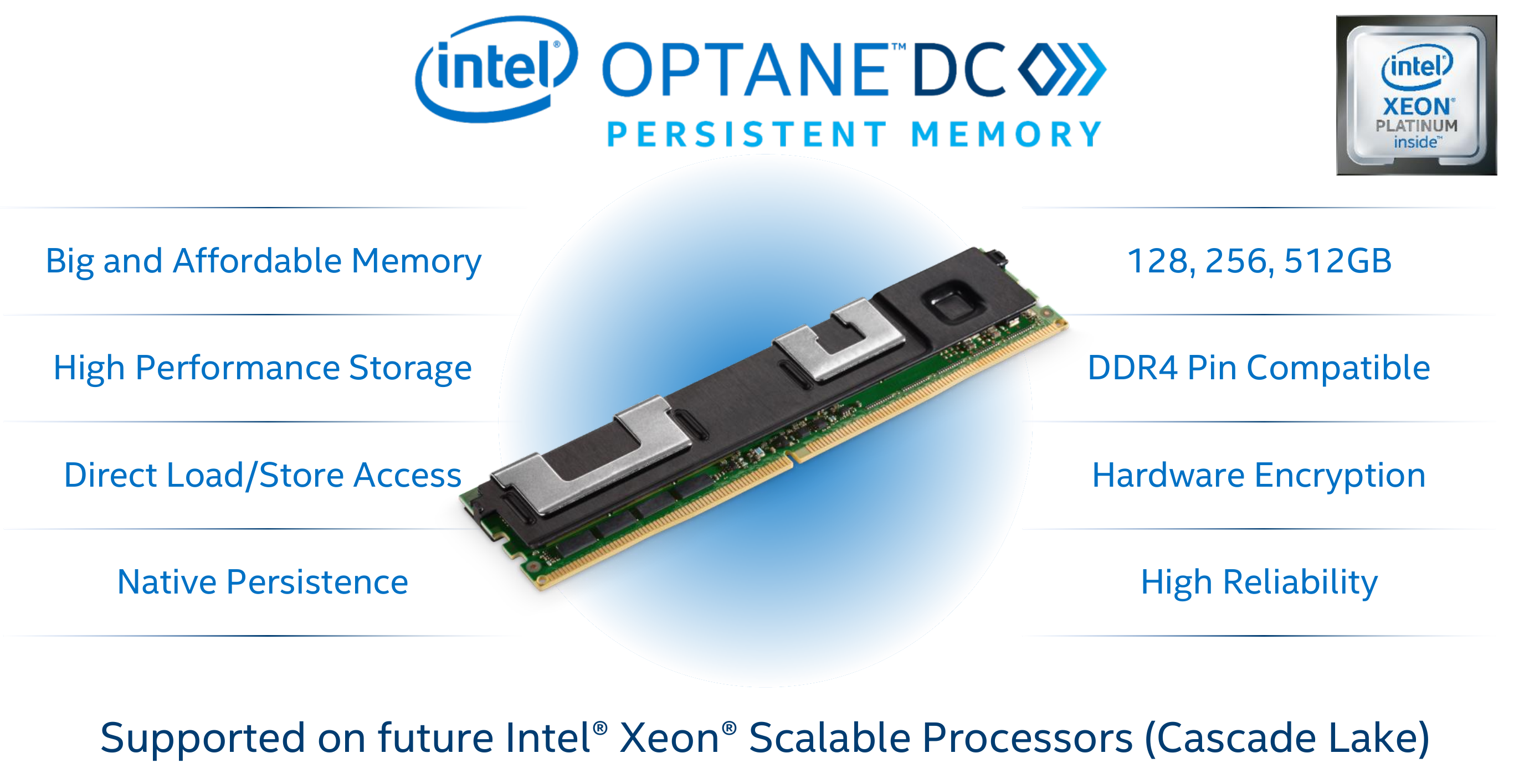
Persistent memory is a hot topic. Data center workloads are not only getting more complex, but they also involve rapidly growing datasets. Recently Intel launched its beta program for Optane DC persistent memory with general availability expected in the first half of 2019. The goal of Optane DC is to offer larger capacity “hot data” or frequently-accessed data such as that typically found in the DRAM.
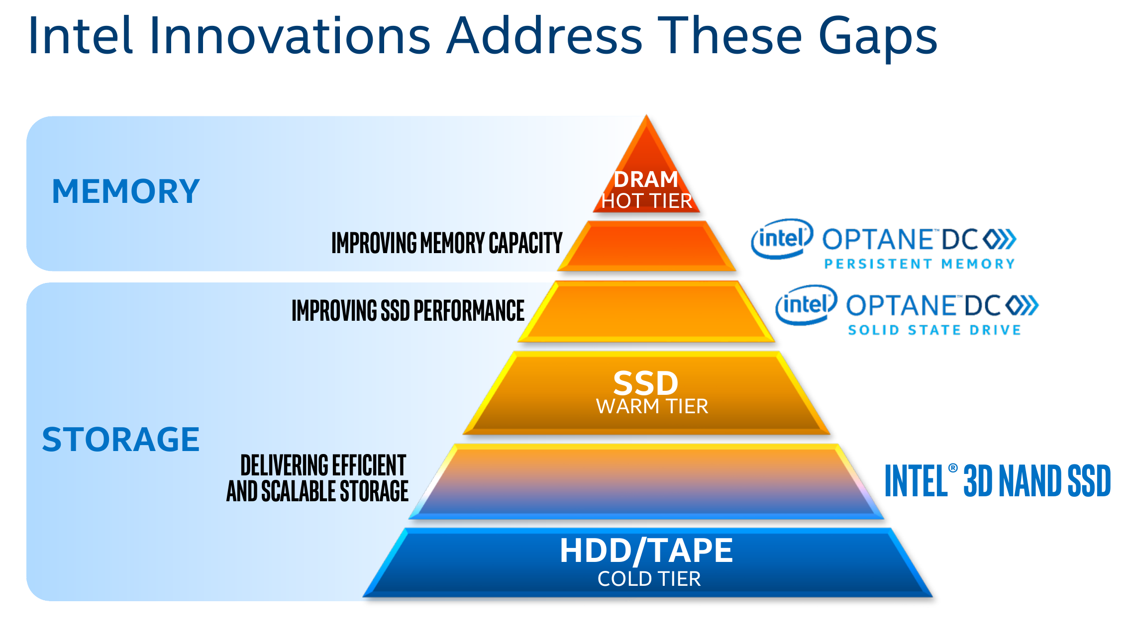
For first-generation Optane DC DIMMs, Intel supports capacities of 128, 256, and 512 GiB. The DIMMs are DDR4 pin compatible and although they are slightly slower than DRAM, they are considerably faster than a typical SSD – fast enough to double up as “slow main memory”. Optane DC DIMMs are designed to work with direct byte-addressable load/store accesses and have built-in encryption. They allow cache line access (i.e., 64B granularity) and offer idle latency close to that of DDR4 DIMMs. At Hot Chips, Intel did not want to disclose much about the encryption mechanism which is necessary due to non-volatility of those DIMMs. Hopefully, more details will come after launch.
Although Optane DC DIMMs are DDR4 pin compatible, meaning they use the same electrical and mechanical interface as DDR4, they are not a direct drop-in replacement. Those DIMMs have different characteristics and therefore they interface with the CPU over proprietary protocol extensions. For this reason, Cascade Lake features an overhauled memory controller capable of interfacing with both DDR4 DIMMs and Optane DC DIMMs. Memory channels can be shared between DDR4 and Optane DC modules. For example, a single channel can have one regular DDR4 DIMM while the other DIMM can be an Optane DC DIMM. All in all, Optane DC DIMMs allow for greater than 3 TiB of system memory per socket.
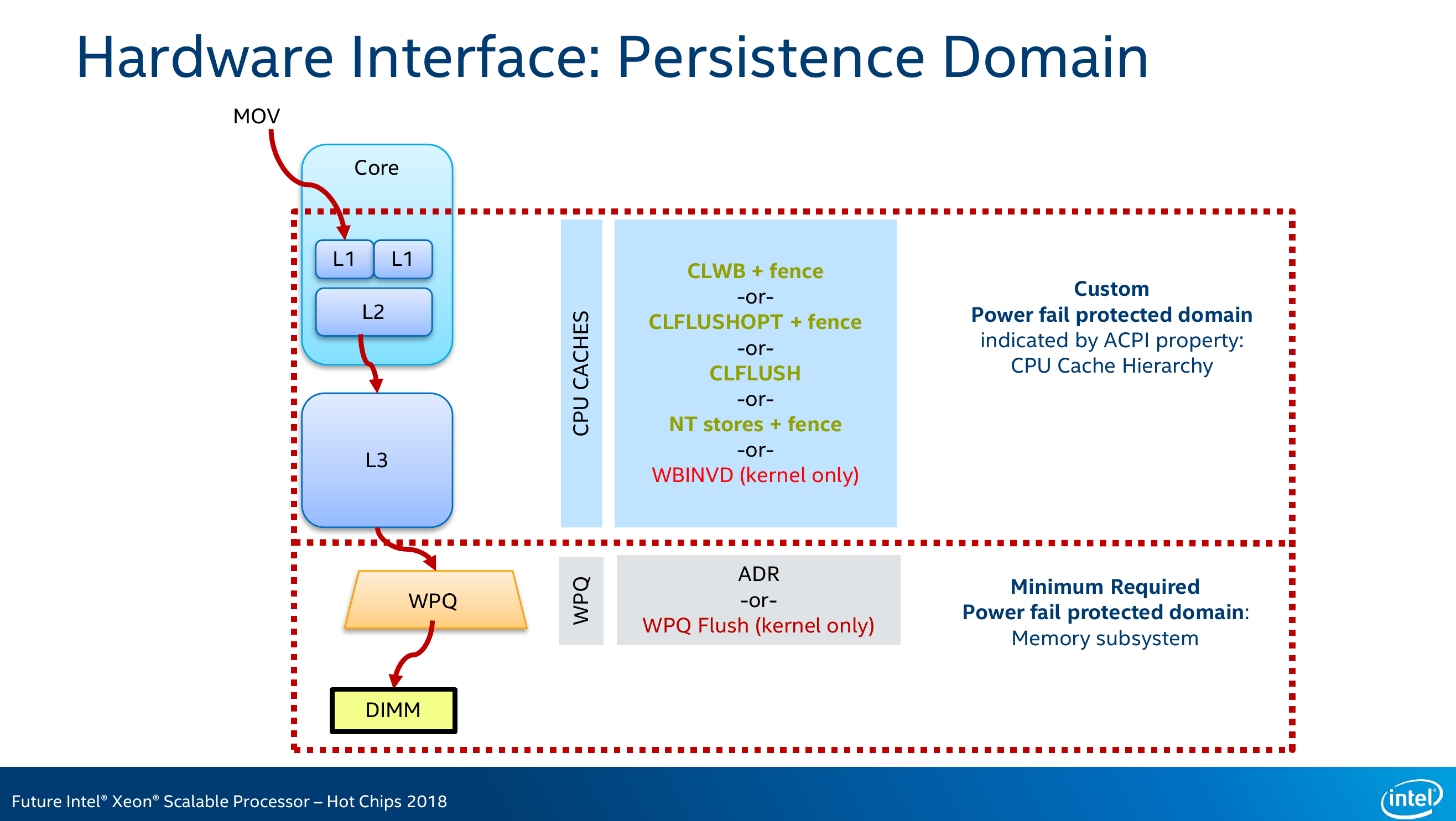
Although the instructions to support persistent memory were already introduced in Skylake, Cascade Lake can now actually make use of them. The bare minimum for persistent memory support can be realized by simply putting the data in the write pending queue (WPQ) of the integrated memory controller within the persistence domain. The persistence domain is a unique checkpoint. Once data makes it to that point, it’s persistence is guaranteed by the platform interface. This is shown below in the bottom dotted box. Any data within that box is either saved on the DIMM, on the way to the DIMM, or in the WPQ in the IMC. Regardless of where it is, the platform is required to store enough energy to save everything within that box in the event of a power loss.
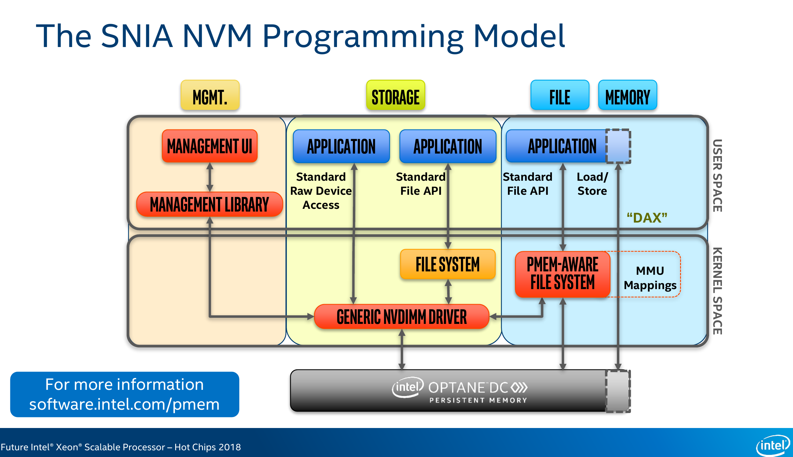
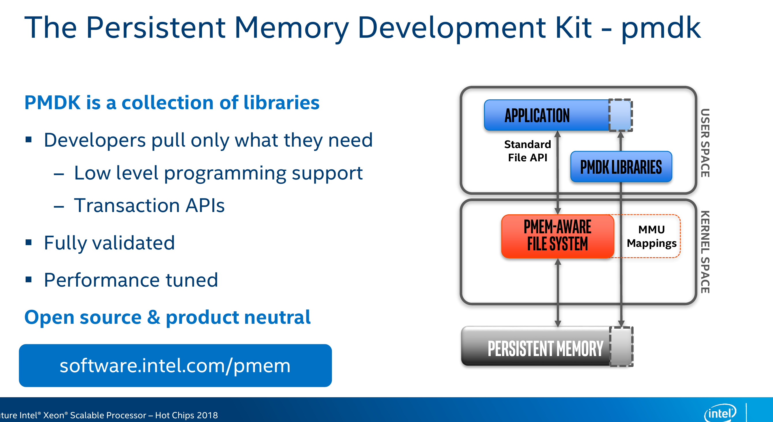
Persistent memory differs from standard DRAM in a great number of ways. Unlike traditional volatile memory which receives an anonymous region of memory, regions of persistent memory are owned by certain applications – much like files on the hard drive. There is a need to keep track of which application has access to which region of the persistent memory which can remain beyond the lifetime of the program’s execution. The Storage Networking Industry Association (SNIA) Technical Working Group (TWG) is the group heading the specification of the persistent memory programming model. The model they have adopted is what’s called a persistent memory aware file system. In other words, use the same standard file semantics the industry has been using for 30-some years and apply it to persistent memory, providing it with the necessary facilities for managing permissions, as well as reading and writing block storage. Additionally, there is also support for mapping memory regions to applications, provides an even more efficient way of accessing persistent memory storage. This feature is also known as direct access or DAX. The quickest way to do this is by simply calling MapViewOfFile()/mmap() which will provide the program with direct load/store accesses. No context switching or interrupts are needed for those accesses. A small caveat to this is that the system is not required to write the modifications back immediately. To ease software support as well as to reduce code overhead required to take advantage of the persistent memory, a number of additional instructions were added which allows programs to flush cache lines within the persistence domain. Intel provides a number of methods to do this. They are briefly listed on the slide above. We will focus on just two instructions: CLFLUSHOPT and CLWB. Both of those instructions were added to facilitate efficient cache flushing. The CLFLUSHOPT instructions, which stands for cache line flush optimized, flushes a cache from all the caches by invalidating it. As its name implies, it is an optimized version of CLFLUSH by behaving similarly but without the serialization, providing some concurrency. The second instruction, CLWB, which stands for cache line write back, flushes cache line but keeps it valid, non-dirty, in the cache. The line is retained, improving the chance of a hit on a subsequent access.
To make working with persistent memory easier, Intel introduced the Persistent Memory Development Kit (PMDK). PMDK is a collection of optimized libraries and utilities for working with persistent memory.
–
Spotted an error? Help us fix it! Simply select the problematic text and press Ctrl+Enter to notify us.
–