
Nvidia Inference Research Chip Scales to Dozens of Chiplets
 We have seen a torrent of new research chips coming out of industry over the past year. New chiplet-based designs and new neural processor architectures are aplenty. Last week we ran an article about an Arm-based chiplet designed by TSMC for HPC which was presented at the 2019 VLSI Symposium. Today we’ll be reporting on another interesting research chip from the symposium – this one is made by Nvidia.
Research Chip 2018 – RC 18
Research chips at Nvidia don’t get catchy codenames. Instead, it’s simply referred to as the 2018 research chip or “RC 18â€. Although the chip was first talked about earlier this year at the 2019 GPU Technology Conference (GTC), the technical details were unveiled earlier this month at the 2019 VLSI Symposium in Kyoto, Japan. The chip was presented by Brian Zimmer, Senior Research Scientist at Nvidia. By the way, we want to point out that semiconductor companies such as Intel and Nvidia routinely design several such research chips yearly for exploratory reasons. It helps them understand which implementations works and what doesn’t work in practice in silicon, why, and what challenges are involved. The knowledge gained from this research is put to work in future products. While companies such as Intel present sometimes as much as a couple of dozen research chips at various IEEE conferences, to see Nvidia talking about one of their internal research chips is quite rare.
This research chip attempts to demonstrate a couple of different technologies:
- Object-oriented logic synthesis
- A fine-grained globally asynchronous locally synchronous (GALS) SoC design
- A die-to-die ground-referenced single-ended serial link (GRS)
- A scalable neural processor accelerator architecture
Note that not everything was specifically talked about. Specifically, the object-oriented logic synthesis aspect of development was not discussed.
One of the relatively unique aspects of a neural processor for inference is the broad spectrum of applications, performance, and power envelope that must be covered depending on the target market. For example, inference in the data center can comfortably be afforded to be done with as many operations per second as possible due to the allowed power budgets that are often in the hundreds of watts. While engineers would love to have such performance in their autonomous cars, power is a formidable obstacle. For that reason, a more balanced performance-power point is often chosen. Likewise, mobile phones have a power budget of just a few watts and on the very end of the scale are edge devices which require prolong battery life with as little as a few milliwatts of power.
Likely, one of the other unique aspects of many neural processors is that assuming they are not memory bound, they tend to scale well with more compute power. The ability to scale lends itself well to a chiplet-based approach. The ability to build multiple systems of varying power and performance requirements using a plurality of a single die is the subject of this research.
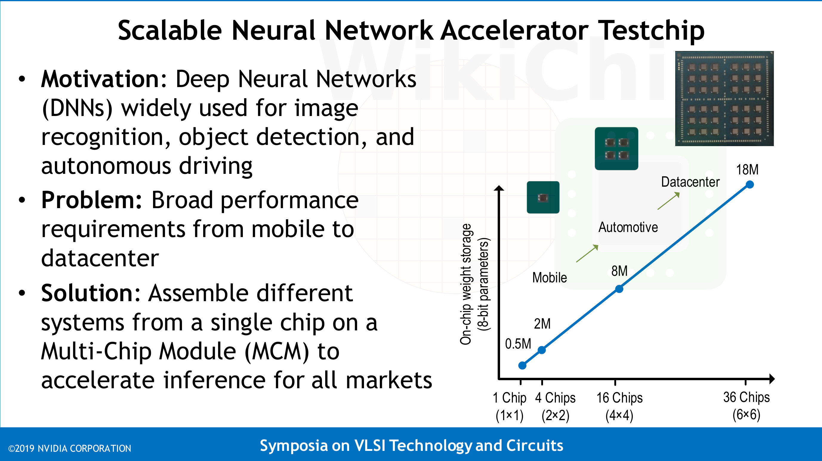
For this research chip, Nvidia decided to scale from a single die up to a 36-die system. Designing such architecture has its own challenges. It must be demonstrated that such a system is capable of scaling from milliwatts to 100s of watts and offer proportional performance scaling at each point along the way. This has to be done with no efficiency loss for both a single die up to the 36-die system. Strong scaling must also be demonstrated in order for larger systems to be able to reduce latency, a critical for areas such as automotive applications.
The Die
From the single-die chip to the 36-die systems, all the dies are identical. Manufactured on TSMC 16-nanometer node, each die occupies exactly 6 mm² of silicon, a modest size by industry standard but sizable, though no enough, for a research chip (this is discussed further later on). On each die is a network of 16 processing elements, a global buffer that stores intermediate activations, the NoC, the NoP, and a management RISC-V core.
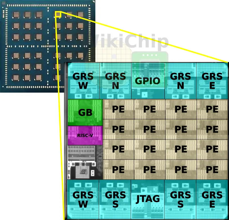
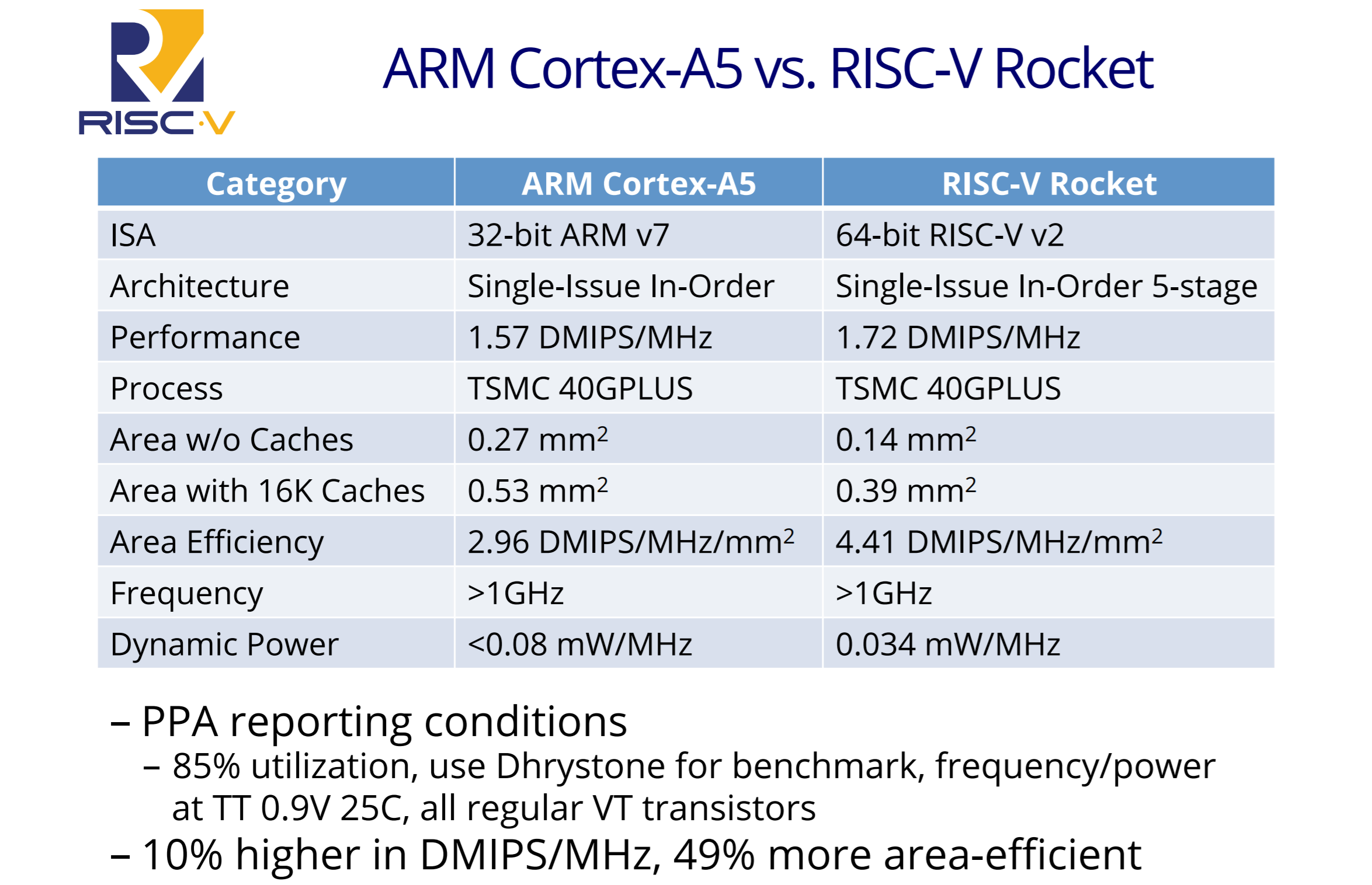
RISC-V Core
The chip incorporates a single RISC-V core based on the open source Rocket configurable core. This is an in-order 5-stage pipeline core comparable to a Cortex-A5 with better area, performance, and power efficiency.
Scaling
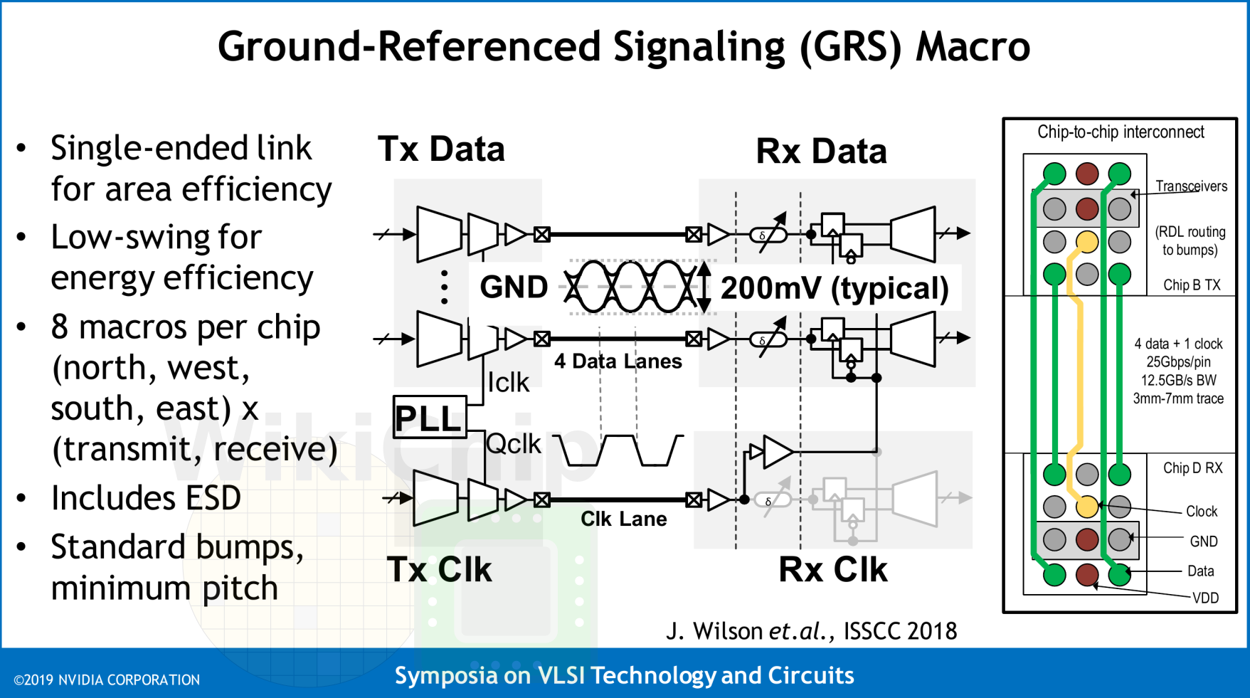
In order to scale the architecture to many chiplets, Nvidia implemented a network-on-package. There are eight Ground-Referenced Signaling (GRS) macros on each die. There is a pair of macros for transmitting and receiving for each compass direction. These macros send or receive 100 Gbps in each of the north, south, east, and west directions.
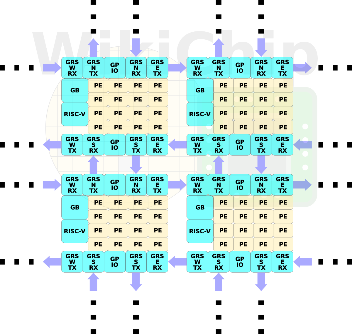
For this research, Nvidia assembled up to 36 chiplets connected together on a single organic substrate. The top six chips have the general-purpose I/O connected to the outside world. The package itself is 47.5 mm by 47.5 mm which is relatively small for the number of dies it’s carrying. It’s worth noting that Nvidia chose a standard organic substrate over some of the alternative packaging technologies such as CoWoS which has better I/O density and bump pitch due to economic reasons. Silicon interposer is simply too expensive for many markets.
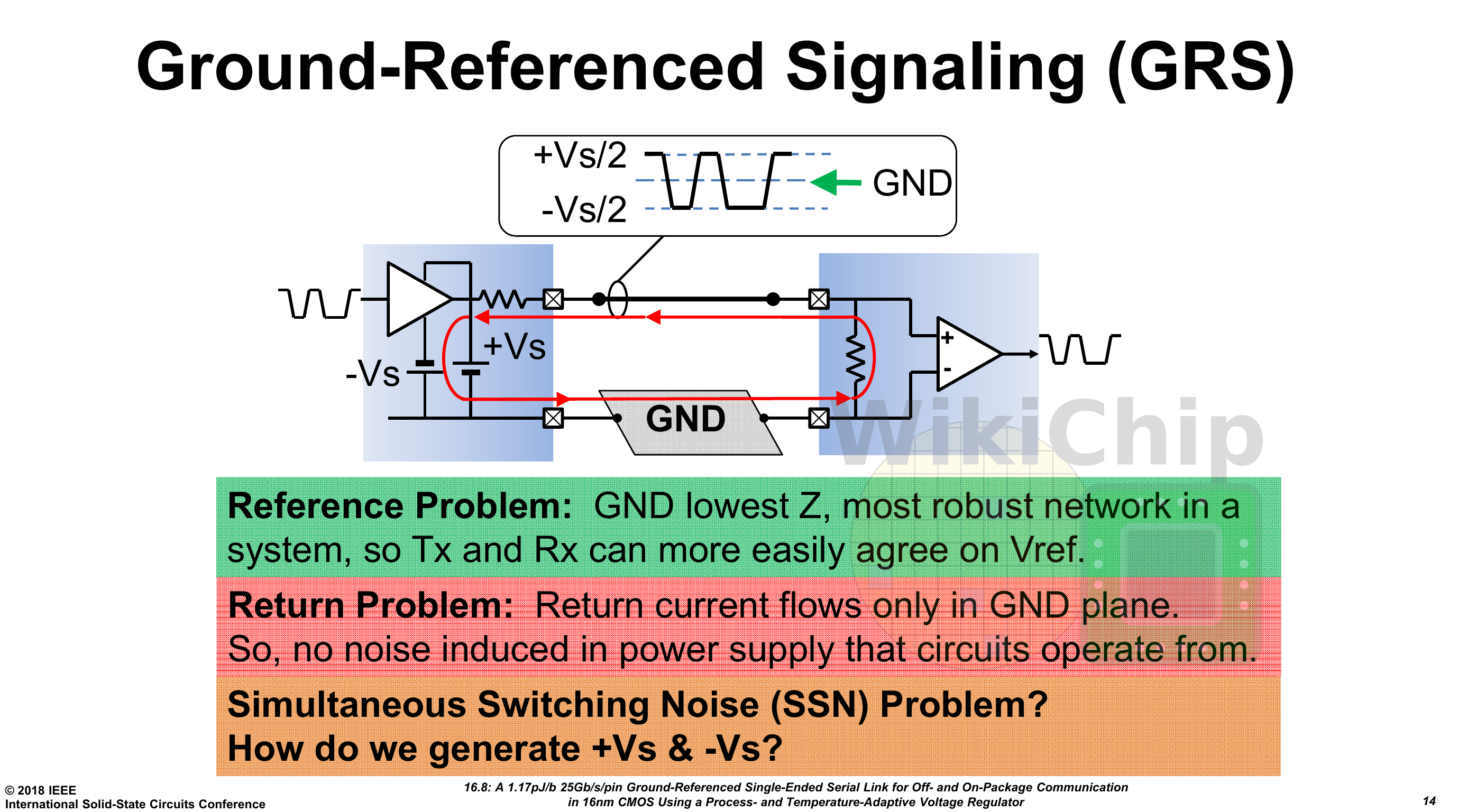
The dies are configured in a mesh topology with large wires that cannot route over die without harming the power delivery. Each macro has a single clock bump and four data bumps. Keep in mind this is using a standard 150 μm bump pitch on a standard organic substrate. Ground-Referenced Signaling (GRS) are single-ended links that are designed to take advantage of conventional inexpensive organic packages and circuit printed boards. Those are short-reach (about 80mm reach) link that uses single-ended signaling. Historically, differential signaling has been preferred for high-speed signaling channels like this due to its inherent noise immunity and lower power characteristics. To overcome some of those issues, especially the ones pertaining to simultaneous switching noise and signal integrity, Nvidia GRS links use the ground as the voltage reference for its robustness and lowest impedance. Return currents flow only on ground and signals are driven symmetrically between the two +Vs and -Vs voltage supplies with respect to ground (in other words, signals are sent either below or above ground). This is low-swing signaling so you’re looking at a peak-to-peak of roughly 200 mV. Clocks are also forwarded.
Loading Data
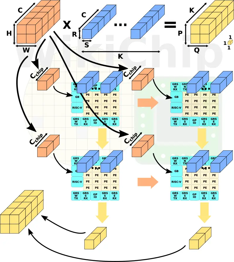
The chip operates on one layer at a time with each layer possibly having a different input and output size as well as predetermined weights. Input is characterized as having a size of H times W with C channels. The input is consequently multiplied by the weight kernel size of R times S with C channels. The output activation size is, therefore, P times Q with K output channels.
The chip then multiplies the R x S x C input elements by the R x S x C weights and finally add all the values together to create a 1x1x1 output. This is repeated P x Q x K times. The inputs are distributed evenly among all the chips. Within each chip, the inputs are then distributed to all the processing elements across the NoC. The top chips ship their outputs to the bottom chips for the accumulation of all C input channels.
–
Spotted an error? Help us fix it! Simply select the problematic text and press Ctrl+Enter to notify us.
–