
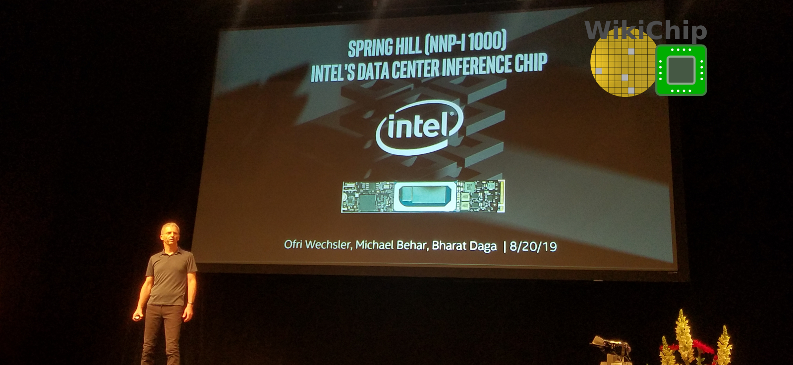
Intel Spring Hill: Morphing Ice Lake SoC Into A Power-Efficient Data Center Inference Accelerator
When Intel disclosed its latest high-performance core, Sunny Cove, they made sure to point out that it will be integrated into a plethora of new products in addition to its traditional server and client SoCs. We have since seen it included in their new 3D integrated product, codename Lakfield and it should come as no surprise when we tell you that they will also be found in their new inference accelerator. But Sunny Cove isn’t the only IP reused in Spring Hill. Intel’s new inference accelerator makes extensive use of the company’s existing IP ecosystem throughout its design. At Hot Chips 31, Ofri Wechsler, Intel’s lead hardware architect at Intel’s Artificial Intelligence Products Group presented their new inference accelerator.
Data Center Inference Acceleration
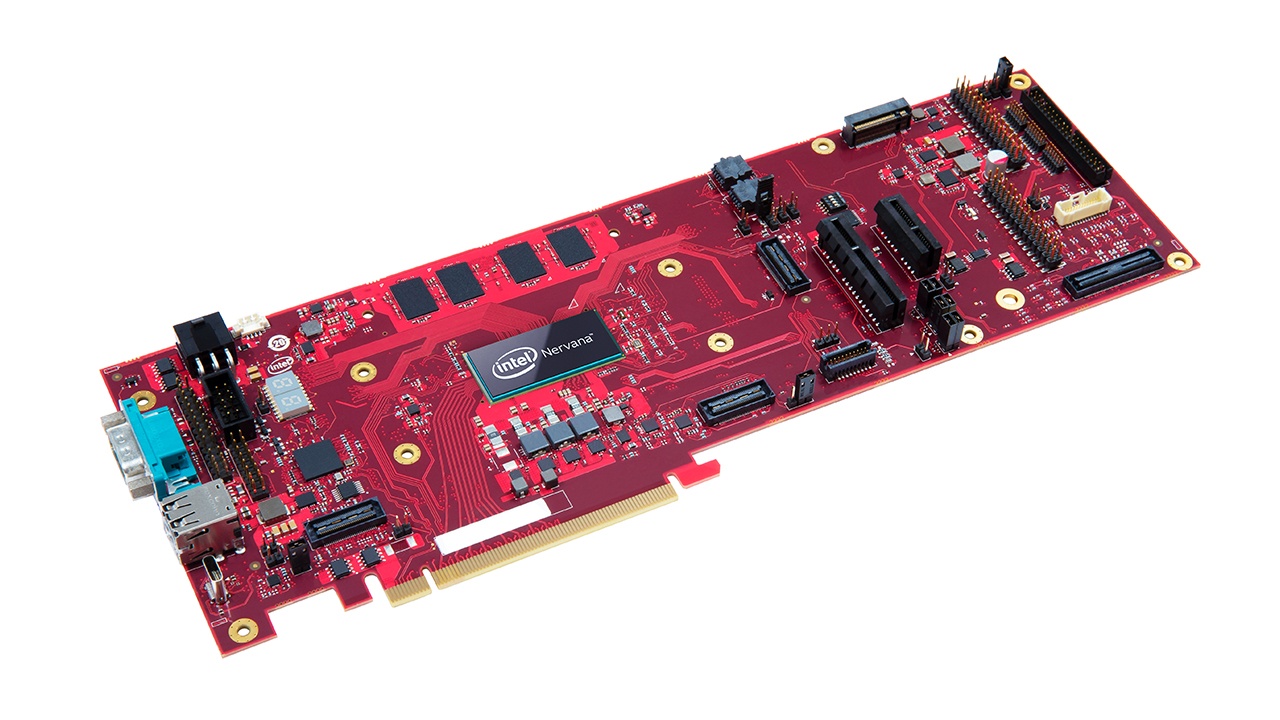
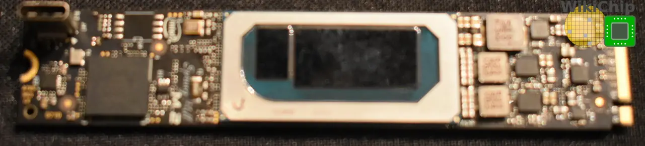
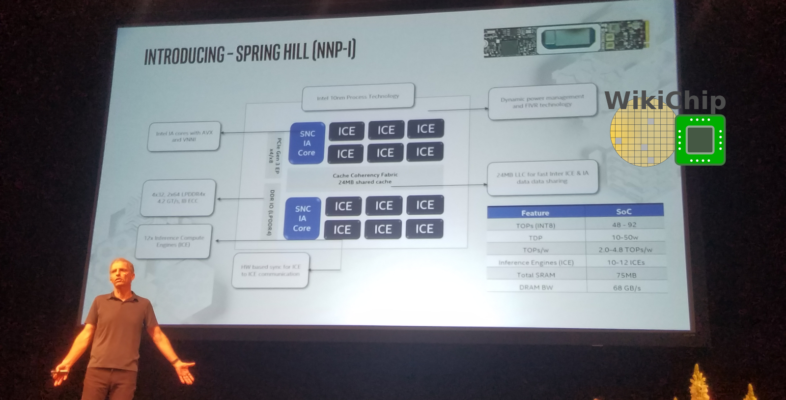
Spring Hill is branded as the Intel Nervana NNP-I 1000 series. Note that the ‘I’ is for inference while the ‘T’ companion series which is based on an entirely different architecture will be for training. It will come in both M.2 and a standard PCIe accelerator card form factors. Intel chose a relatively low TDP ranging from 10 to 50 W in order to ease migration without the need for additional power and cooling requirements per node/rack. By comparison, a relatively low-power GPU aimed for inference such as the T4 is 70 watt. The low power envelop makes sense for an M.2 product (albeit, the entire range is already very high for M.2 and cooling will be challenging), but given this is a data center product, 50 W just doesn’t feel ambitious enough. Intel isn’t ready to talk about the PCIe cards just yet, but you can find an illustration of it on its website. It’s possible we might see higher power consumption with those cards in the future but that remains to be seen. The M.2 board, which is shown below, connects to a host CPU via a 4x PCIe.
Over the Icy Lake to the Spring Hill
We noted earlier that Intel reused existing IPs extensively throughout Spring Hill. Actually, the base SoC for Spring Hill is Ice Lake. At a 5000-feet view, fabricated on Intel’s 10-nanometer process, Spring Hill borrows the LPDDR4x interface and memory controller, the system agent and power management (including the FIVR), the PCIe interface, and kept two of the Sunny Cove cores along with the ring interconnect. To that end, the SoC supports up to x8 PCIe Gen 3 (although note that Intel’s own site displays an illustration of an x16 PCIe card based on the NNP I). Additionally, just like Ice Lake, Spring Hill also supports quad-channel (128b I/F) 32b LPDDR4x-4200 for a bandwidth of up to 67.2 GB/s with a maximum memory capacity of 32 GB of DRAM.
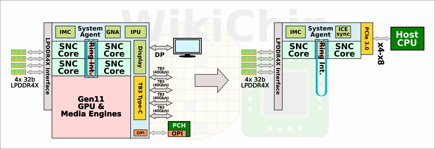
The remaining cores and the Gen11 GPU have been removed. Instead, Spring Hill integrates 12 new Inference Compute Engines (ICEs). Each SNC core comes with its own 3 MiB LLC slice of cache while the ICEs are integrated as duplexes with their own 3 MiB of LLC slice. In total there is 24 MiB of last level cache comprising eight LLC slices. Interestingly, Ice Lake, as with prior Core generations, continues to integrate 2 MiB of cache per LLC slice while Intel’s next-generation SoC, Tiger Lake, appears to move to 3 MiB of LLC slices.
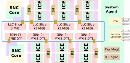
The two large cores have a couple of different jobs. First and foremost they are there to execute the AI compiler runtime code which orchestrates the handling of all the applications on the SoC. The host CPU offloads the entire workload to the Spring Hill accelerator. The big cores setup the application across the appropriate number of ICEs along with the way communication flows and executes the job. When complete, the results are sent back. By the way, part of the reason Intel went with the big x86 cores is to simplify software migration from their Xeons to the NNP-I’s. It’s worth adding that since the two cores are full-fledged Sunny Cove cores with AVX-512, VNNI, and all the other extensions, for flexibility, developers may choose to leverage those cores to do any other desirable processing.
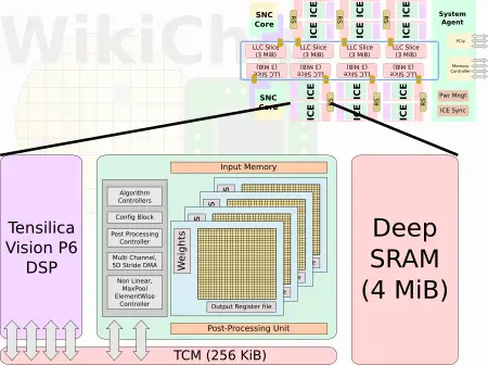
The Inference Compute Engines (ICEs) are the workhorse processing units of Spring Hill. Each ICE comprises a large 4 MiB SRAM pool, 256 KiB of high-bandwidth tightly-coupled memory, a Tensillica Vision P6 DSP, and a DL compute grid. With 12 ICEs you are looking at 48 MiB of additional deep SRAM memory on top of the 24 MiB of LLC.
The TCM block is interlinked to both the DSP and the Compute Grid. Spring Hill incorporates hardware synchronization logic designed to simplify ICE-ICE, ICE-SNC, and ICE-Host communication. Workloads may be optimized for throughput by allocating few ICEs per applications, or for latency by combining many ICEs for a single workload. Intel mentioned the ability to attach multiple accelerators to a single host CPU, but spanning workloads across multiple accelerators does not appear to be supported. At least not with this first generation.
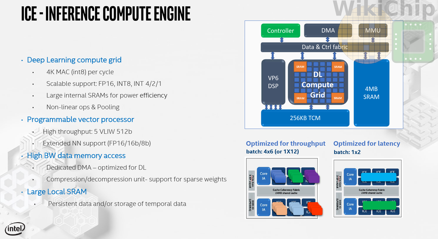
Intel targeted 5 TOPs/w with Spring Hill. To get there you need a highly optimized logic for computing the models. This is where the custom DL Compute Grid comes in. The grid itself comprises 4K 8b MACs. Wechsler noted that it has been designed to very efficiently handle lower precision (such as INT 4, 2, and even 1). To maximize data reuse, the grid is organized as a 4D structure (presumably 32x32x4) with input data getting broadcasted across the entire grid simultaneously. The exact layout mapping of the layers is determined by the compiler at compile-time which can perform various transformations to better utilize the hardware. The compute grid hardness various functions and comes with the ability to perform various more complex operations.
Where the DL Compute Grid falls short or for any new operation, each ICE also comes with a customized Cadence Tensilica Vision P6 DSP. This is a pretty beefed up 5-slop VLIW DSP which has been confirmed with two 512-bit vector load ports. It supports FP16 as well as 8-32b integer operations. Intel says that they have customized the DSP with an additional set of custom instructions that would be needed for the acceleration of some of the more unique neural network models and functions.
All in all, Spring Hill will come in a number of different SKUs from 10 to 50 W and 10 to 12 ICEs for a total of 48 to 92 TOPs (8b). This works out to power-efficiency of 2.0 to 4.8 TOPs/w which is very close to the hard target they desired. It’s also considerably higher than anything on the market today. The only thing that currently gets close is Tesla’s FSD but their figure is for the NPUs alone whereas Intel’s figure is for the entire SoC (albeit not the entire package which includes the PCH). By the way, it’s worth noting that it’s actually unclear what’s included in that number. In addition to the DL Compute Grid which offers a peak performance of 4096 OPs/cycle/ICE, the P6 DSP itself can do 256 OPs/cycle/ICE. Nonetheless, a ballpark estimate suggests the SoC will be clocked as high as 1.8 GHz. Wechsler also suggested that the compiler is capable of doing some of the frequency and power determination/allocation for the ICEs at compile time but didn’t go into too many details. It’s worth pointing out that since Spring Hill makes use of Ice Lake DVFS power management circuits and FIVR, we might see very fine per-ICE frequency control similar to Intel’s Turbo Boost Technology found in all Intel CPUs. Many data center inference jobs also tend to be quite sporadic. The ability for ICEs to go into a temporarily high boost frequency in order to drastically improve latency could prove advantageous.
Intel promises preliminary performance numbers when the MLPerf 0.5 Inference Benchmark gets published (November 6th). Intel said that there are two more generations already in development. The product is currently sampling with volume production expected to start by the end of the year.
WikiChip microarchitectural page: Spring Hill.
–
Spotted an error? Help us fix it! Simply select the problematic text and press Ctrl+Enter to notify us.
–