
A Look At Qualcomm’s Data Center Inference Accelerator
About four years ago Qualcomm attempted to enter the data center market with its own Arm-based server CPUs with the launch of the Centriq 2400 server family based on their custom Falkor microarchitecture. Within less than a year after its launch, the company canned its data center effort. Now, Qualcomm is heading back into the data center. But instead of fighting over CPUs, the company is going after the rapidly growing AI market. The company hopes its expertise in AI inference acceleration in the mobile market will allow it to efficiently scale to the data center.
Cloud AI 100
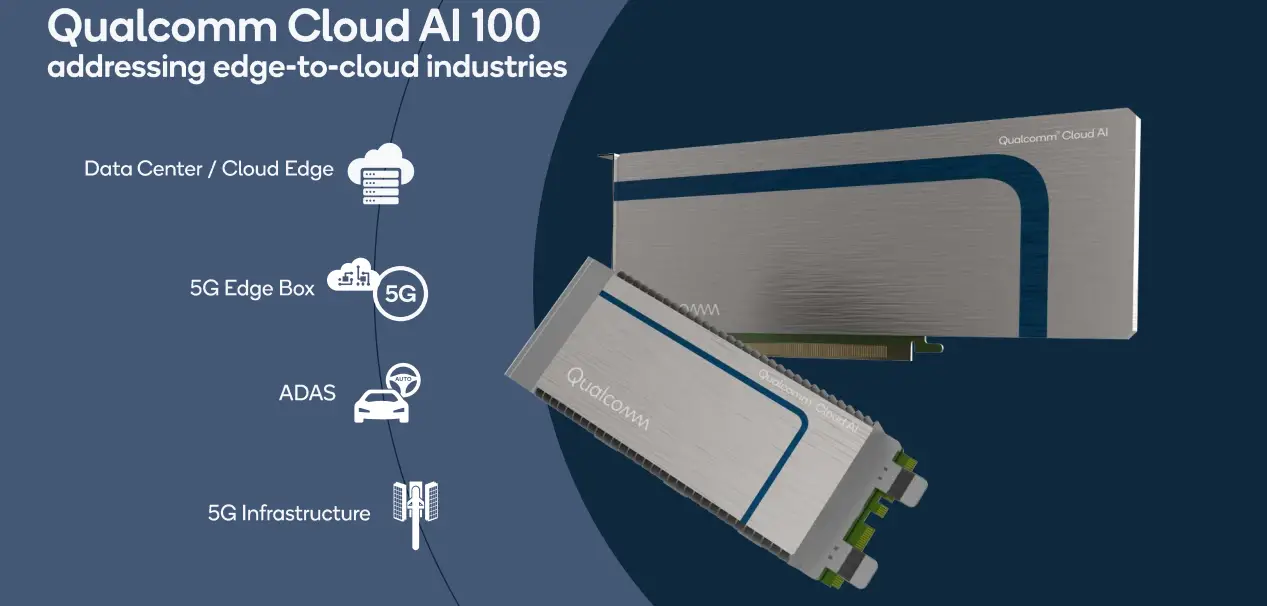
Qualcomm’s first series of inference accelerators is called the Cloud AI 100. “We are currently actively collaborating with several industry leaders for deploying this solution,” said Karam Chata, Lead Engineering Team for Cloud AI 100 at Qualcomm. It is designed to span from the data center down to the edge devices. Three different form factors have been announced: a PCIe card for data center servers with TDPs of up to 75 W, a dual M.2 module with mid-range performance, and TDPs of 15-25 W, as well as a dual M.2e module with no heat sink for embedded devices. Each product features roughly half the performance (OPs) of its bigger version with the data center PCIe card maxing out at 400 TOPs (Int8) and 200 teraFLOPs (FP16). We will delve a bit deeper into those products later on in this article.
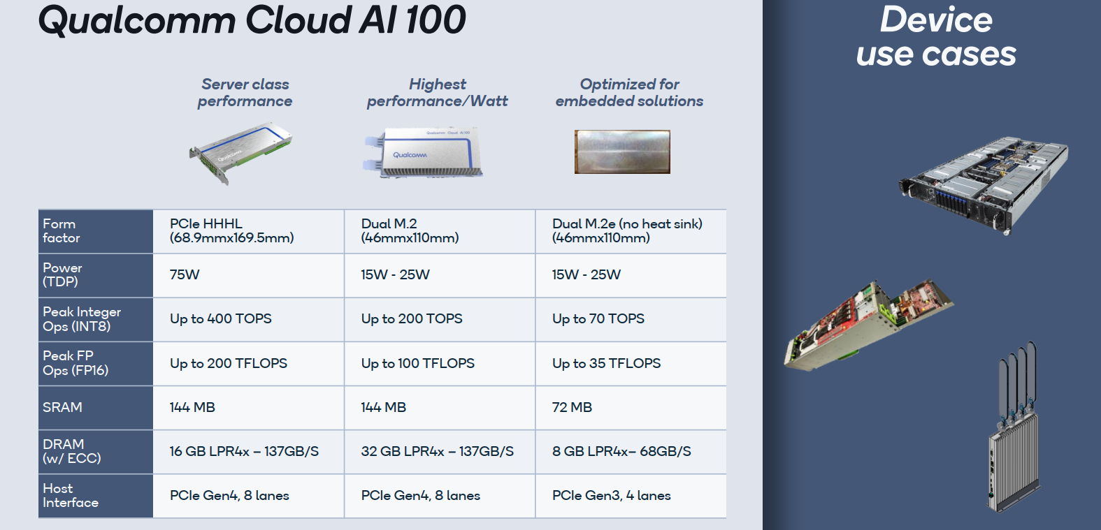
One thing to point out with those three products is that the Dual M.2 variant with the heat sink actually has twice as much memory as the PCIe card. This is despite offering half the peak theoretical compute as the PCIe card. Note that the bandwidth remains identical for both devices at 136.5 GB/s.
SoC
The chip itself is a single die fabricated on a 7-nanometer process. The underlying SoC architecture is a homogeneous multi-core design. There are 16 ‘AI Cores’ interconnected via a high-bandwidth NoC. Unlike some of the other inference accelerators out there, there are no additional specialized components outside of the cores. Likewise, there is also no large shared memory pool at the SoC level. All computations take place within the AI Cores which includes both a large amount of memory and compute logic.
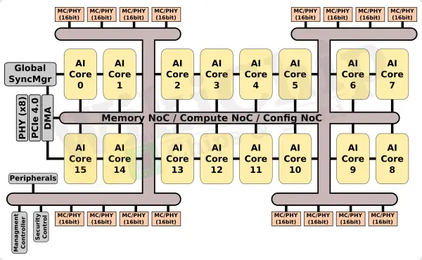
Supplementing the on-die memory, the SoC integrated a 256-bit wide LPDDR4x interface supporting rates up to 4266 MT/s for a bandwidth of 136.5 GB/s. The embedded devices variant appears to offer half of that (68.26 GB/s), presumably due to a narrower 128-bit-wide interface. As far as the host interface goes, the SoC supports x8 lanes of PCIe 4.0.
The overall design is similar to other chips on the market. For example, Baidu’s accelerator also incorporate 16 compute units (half specialized, half generalized) on a NoC. Intel’s Spring Hill (now discontinued) incorporated 12 compute engines along with 2 general-purpose x86 cores. Habana’s Goya also features tens Tensor Processor Cores (TPCs) on a NoC. Both Baidu’s Kunlun and Habana’s Goya integrate a large shared memory pool outside of the cores/EUs whereas Qualcomm’s AI 100 and Spring Hill incorporated a large amount of distributed memory within the cores/EUs.
AI Core
Workloads are distributed among the sixteen AI Cores. “The cores are derived from our mobile solutions, however, we’ve upped the performance capabilities to address the cloud and edge workloads,” said Chata. The core is a multi-threaded 4-way VLIW architecture along with a private L1 cache and a large 1 MiB L2 cache. Each core also incorporates a large 8 MiB of tightly-coupled memory designed to reduce DDR memory movement. This means that for all sixteen cores on the SoC, there is a combined of 144 MiB of on-die SRAM. Revisiting the product table we showed earlier, both PCIe and the Dual M.2 support the full amount while the embedded variant appears to feature half of that – 512 KiB of L2$ and 4 MiB of TCM.
This vector TCM memory is designed to store things such as weights and is accessible by the scalar unit, vector unit, and tensor unit within the core. If we’re dealing with 8-bit quantized-value weights, this translates to around 150M weights for the whole chip. Qualcomm says that the scalar processor supports over 1800 instructions with the vector unit supporting another 700+ instructions for AI, CV, and image processing. Both units support 8/16-bit integers as well as 16/32 floating-point values. The vector unit supports up to 512 Int8 MAC/clock as well as FP16 at half-throughput at 256 FP16 MAC/clock. At the SoC-level with all sixteen cores fully utilized, this equals 16 KOPS/cycle (or 8 KiloFLOP/cycle for FP16).
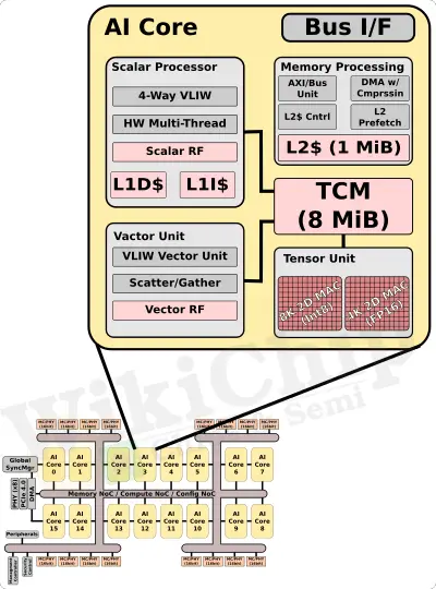
Each core integrates a specialized tensor unit as well to maximize performance/watt. It supports Int8 and FP16 MAC operations. Each tensor unit is capable of up to 8K Int8 MACs/clock and up to 4K FP16 MAC/clock. With 16 cores on each SoC, you’re looking at a pretty sizable compute power – 128 KMAC/cycle (Int8) and 64 KMAC/cycle (FP16). Qualcomm advertises its chip as capable of up to 400 TOPs (Int8) and 200 TFLOPS (FP16). If we assume that number is derived solely from the tensor unit, it means that the AI 100 supports frequencies of up to around 1.5 GHz.
All sixteen cores are interconnected with a number of NoCs. If we use our 1.5 GHz peak frequency estimate again, it appears that the NoC is 1024-bit wide, yielding a bandwidth of 192 GB/s (Qualcomm claimed the inter-AI Core NoC had a bandwidth of 186 GB/s).
Power Claims
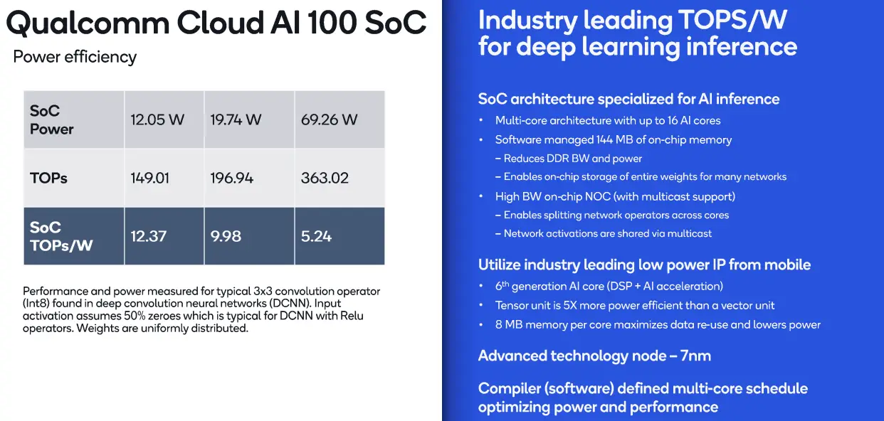
At Hot Chips 33, Qualcomm presented some power efficiency numbers at three different power levels for edge through the data center. The performance claims are not based on a certain model but rather based on an Int8 3×3 convolution operation with uniformly distributed weights and input action comprising 50% zeros which Qualcomm says is typical for Deep CNN with Relu operators. To that end, Qualcomm says the AI 100 can achieve up to ~150 TOPs at ~12 W at over 12 TOPS/W in edge cases and ~363 TOPs at under 70 W at 5.24 TOPs/W in data center uses. Numbers are at the SoC level.
At Hot Chips 33, Qualcomm presented some additional performance results based on the MLPerf benchmark/datasets.
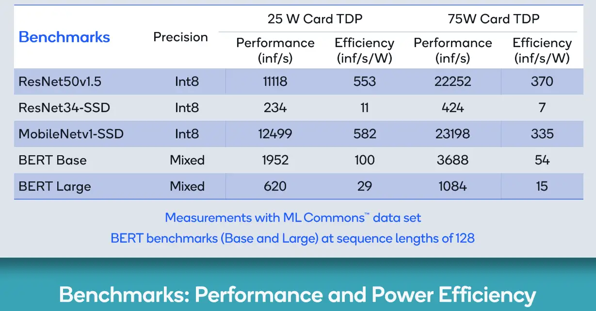
In April, MLPerf leased v1.0 Inference: Edge results. In the ‘closed division – power’, the AI 100 fared incredibly well against the Nvidia Xavier. For ResNet (Offline), the Xavier achieved ~1100-1400 samples/s at 20-25 W while the AI 100 (using the Dev Kit) scored ~5000-7800 samples/s at 28-36W. Likewise, in image detection, the Xavier achieved ~30 samples/s at ~20W while the AI 100 achieved ~93-160 samples/s at 27-36W. Note that the power is system power for all scores.
Availability and Scalability
Qualcomm started sampling its Cloud AI 100 late last year and is available to lead customers since earlier this year. Qualcomm offers a ‘Cloud Edge AI 100 Development Kit’ which comprises a Snapdragon 865 SoCs along with the Cloud AI 100 Dual M.2e module along with the X55 5G Modem. The development offers 50 TOPs of AI compute at 15 W TDP.
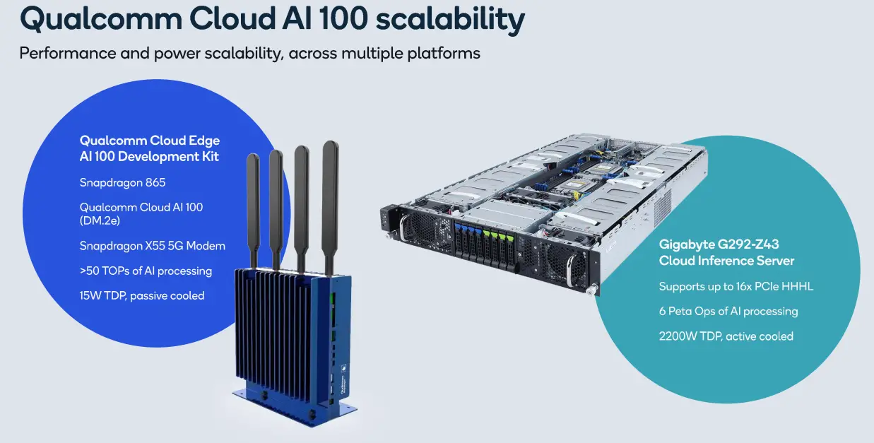
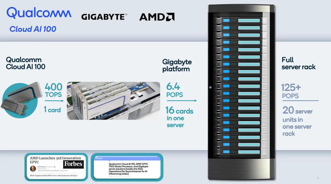
Additionally, Gigabyte also offers an ‘AI-focused’ G292-Z43 2U server with 2 AMD Milan CPUs along with 16 Qualcomm Cloud AI 100 cards for up to 6.4 petaFLOPS (FP16) of compute per server (or 120 petaFLOPS per rack).
–
Spotted an error? Help us fix it! Simply select the problematic text and press Ctrl+Enter to notify us.
–