
TSMC Digs Trenches In Search Of Higher Performance
Greater challenges loom as designer gear up for upcoming 5-nanometer and 3-nanometer nodes. The miniaturization of devices on modern integrated circuits resulted in challenges for circuit designers dealing with power and ground distribution networks (PDNs). The last decade saw the rise of FinFET devices, bringing higher drive strengths compared to prior planar devices. The use of FinFET devices increases the drive strength per unit area, meaning higher current densities and larger current transients. This trend has resulted in chips that are increasingly sensitive to fluctuating supply voltages, exacerbating the power integrity challenges of system design. Circuit designers rely on decoupling capacitors as a fundamental tool for reducing the impedance of PDNs, suppressing noise and improving the overall PI by decoupling or bypassing one part of an electrical circuit or interconnect from another. For signals, noise from the interconnect can be shunted through a decoupling capacitor before being passed to another circuit. But to this well, parasitic resistances and inductances must be kept in check which typically means decaps must be physically located in close proximity to the desired circuit.
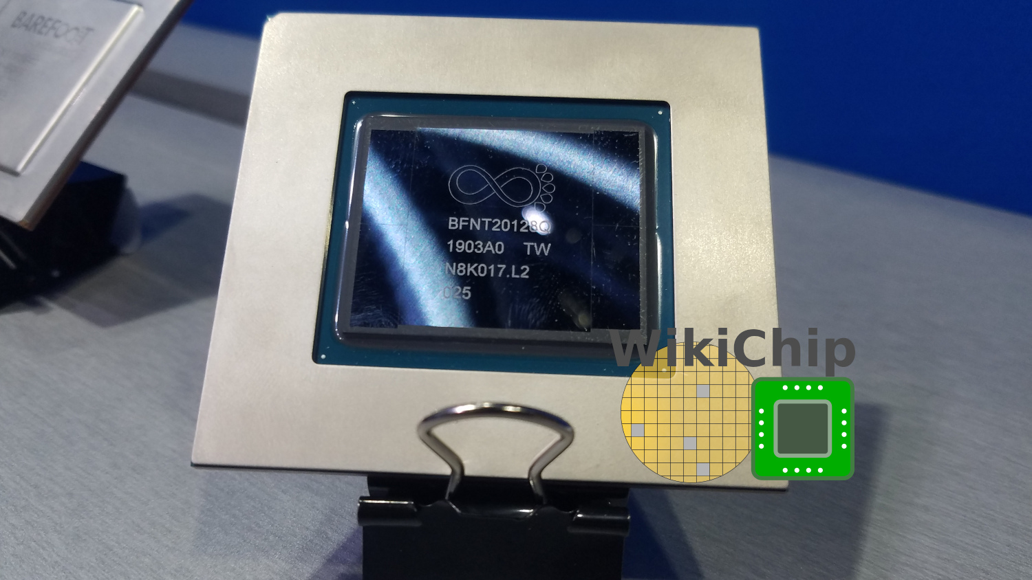
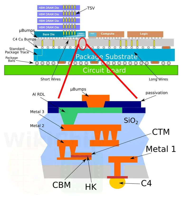
TSMC’s main packaging product for high-performance computing applications is Chip-on-Wafer-on-Substrate (CoWoS). This 2.5D wafer-level system integration is used to efficiently integrate multiple dies onto a silicon interposer. The use of silicon enables very fine sub-micron interconnects. Additionally, it also enables the use of much smaller micro bumps, which allows higher signal density and thus higher bandwidth at lower energy per bit, making it desirable for high-performance chips. CoWoS is used in a wide range of products including GPUs, CPUs, vector processors, neural processors, and programmable switches.
In order to help reduce signal noise and ensure stable voltages, TSMC took advantage of the silicon substrate that already exists in the package to implement high-density metal-insulator-metal (MiM) decoupling capacitors which could potentially be used to replace or assist some of the bigger discrete MLCC components you would otherwise have to mount on top.
At IEDM 2014, TSMC described the new HD-MiM. The high-K MiM was inserted between the Metal1 and Metal2 layers of the Si interposer. Since they are right in the interposer, they can effectively be used for system-level decoupling applications. At the time 1-, 2-, and 3- in-series decap combinations were discussed which provided a capacitance of 17.2, 4.3 and 1.9 fF/µm² respectively. With the HD-MiM, over an entire capacitor area of 200 mm², the HD-MiM can achieve a total capacitance of about 3.5 μF for the interposer die.
Deep Trenches
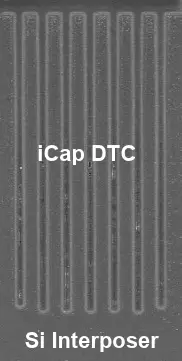
Future high-performance circuits demand even better decoupling capacitors to mitigate droops and absorb transients. At the 2019 IEDM which was held earlier this week, TSMC introduced iCAP. iCAP takes a radically different approach – instead of going horizontally, TSMC has chosen to go vertically with deep trenches. The first time we’ve seen TSMC take this approach was a few years ago with the introduction of Apple’s A10 processor which used the InFO package along with Through InFO Via (TiV). There, TSMC replaced the MLCC LSCs and similar components with DTCs in order to significantly increase the capacitance density possible.
Since both TSVs and DTCs co-exist on the same silicon wafer, there are two ways to construct iCAPs. In the DTC-first approach, the deep trenches are formed prior to the TSV process which means special care must be taken to ensure the TSV thermal budget does not impact the DTCs. Alternatively, in a TSV-first flow, the TSV structures are formed first using the standard TSV process, but special care must be taken to mitigate TSV related issues such as the via protrusion phenomenon. Like HD-MiMs, a major benefit of DTC over package decaps is that they can be freely placed as close as possible to the desired circuit similar to on-chip decaps but with the added benefit that the deep trenches allow for much higher capacitance. Additionally, since this can be implemented across an entire 1700 mm2 interposer with all kinds of chips on top, the DTCs can be more finely designed to better address the PI of the chip above it.
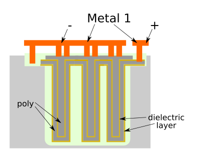
The iCAP standard cell is 40 µm by 40 µm. While TSMC was unwilling to disclose the depth of the trenches, the capacitance density it is able to achieve is up to 340 nF/mm². This translates to close to 20x improvement in capacitance density over the HD-MiM. Since multiple iCAPs can be used on a single interposer, the total capacitance possible is over 68 μF per Si interposer.
Both the HD-MiM and iCAPs are high-yielding and have reported leakage currents below 1 fA/μm², including at high temperatures. TSMC reported very good PDN improvements with iCAP. Compared to equivalent CoWoS-based design without iCAP, TSMC is reporting just 0.05x the impedance and 0.45x the voltage droop.
–
Spotted an error? Help us fix it! Simply select the problematic text and press Ctrl+Enter to notify us.
–