
Intel Launches 3rd Gen Ice Lake Xeon Scalable
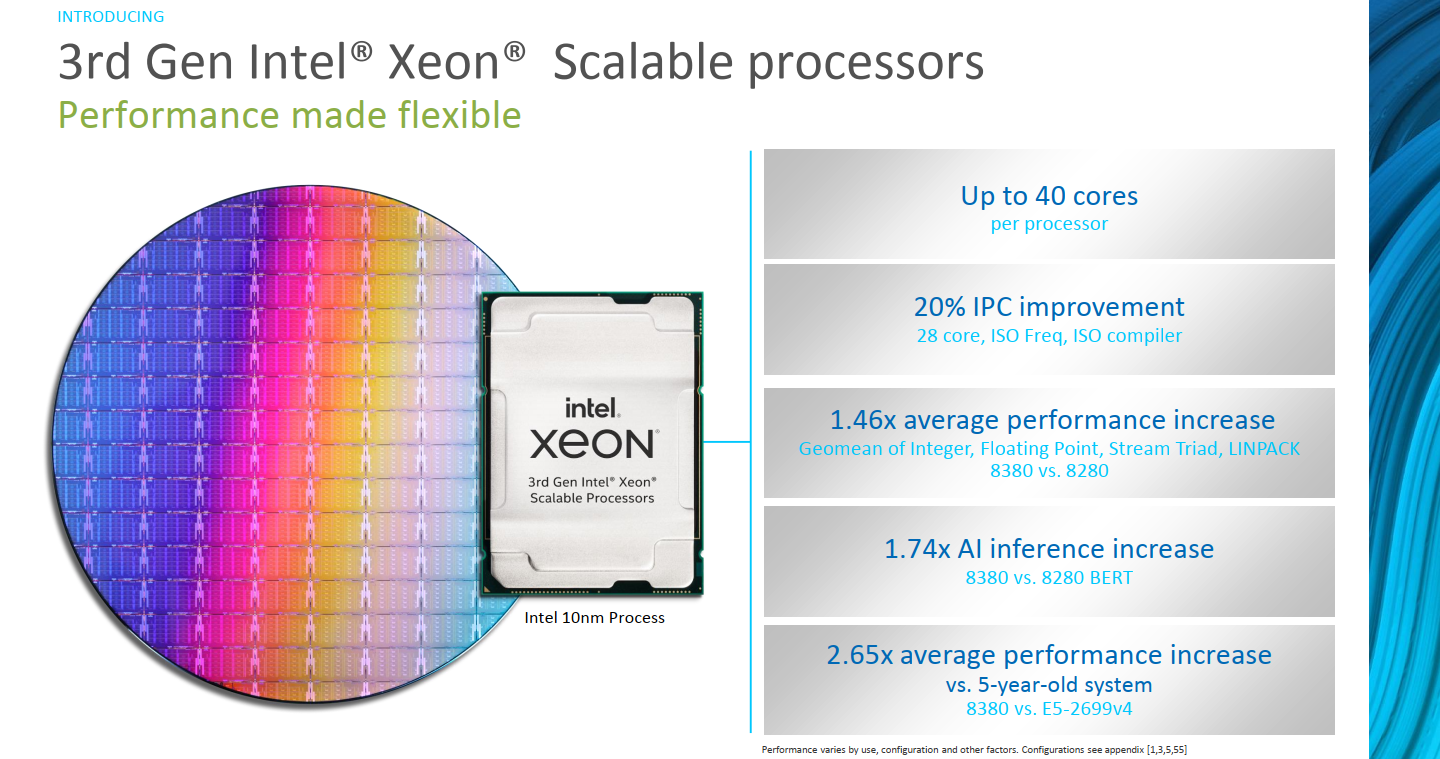
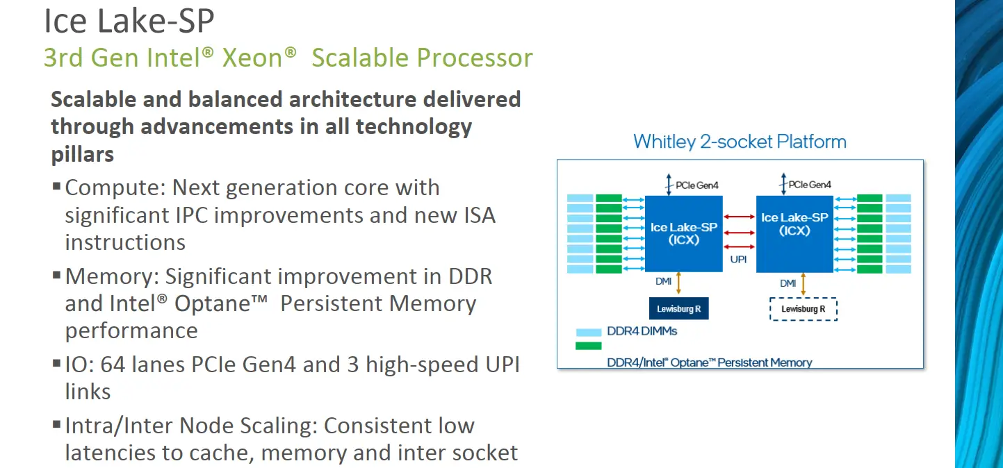
Today Intel is launching its 3rd-Generation Xeon Scalable server processors. Codenamed Ice Lake-SP, these are the first series of server processors fabricated on the company’s 10-nanometer process. Ice Lake server chips are part of the 2-socket Whitley platform which introduces a number of new platform-level improvements in addition to the SoC itself.
Ice Lake
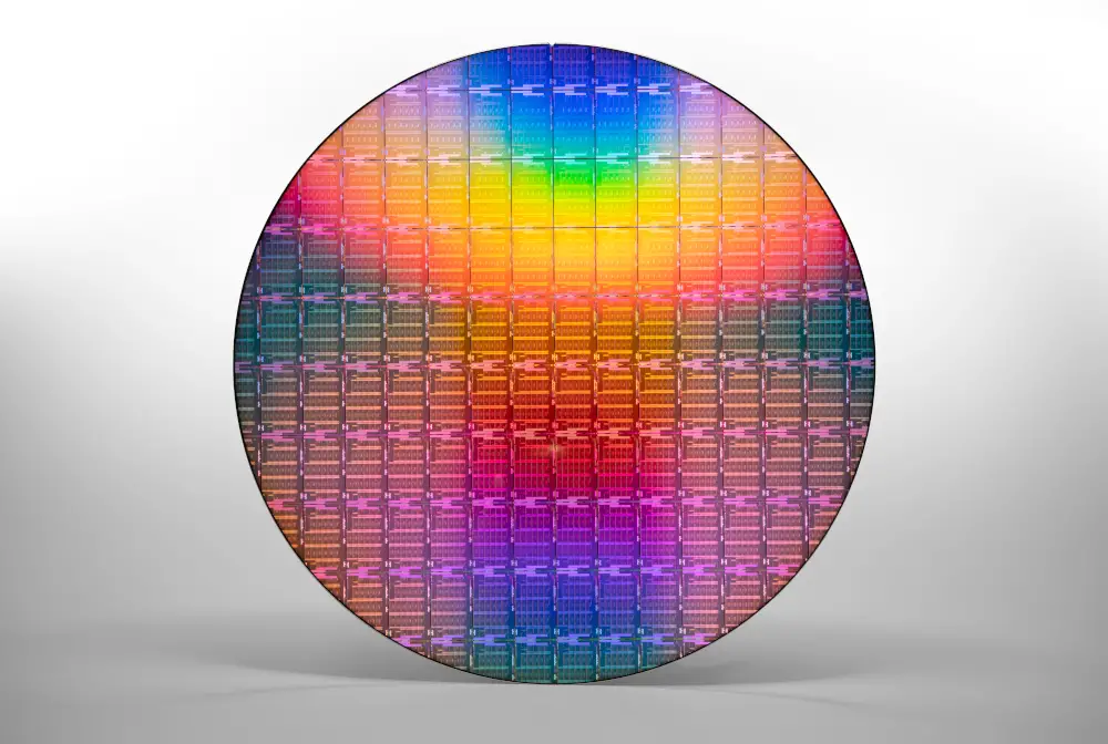
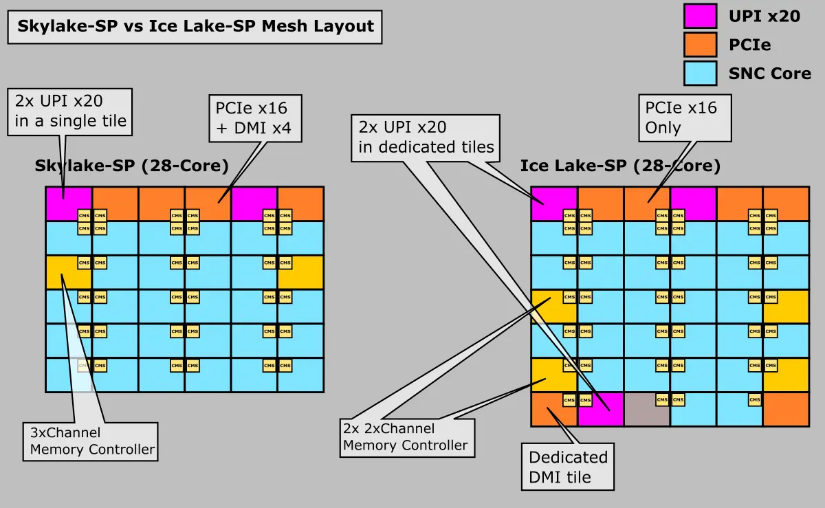
The Ice Lake SP SoC is fabricated on the company’s 10-nanometer process. These are the first server parts to use this process. When Skylake SP was first introduced, it was said that modularity was one of its main design goals – the ability to add more cores and more I/O in the future was baked into the original design. Ice Lake server processors largely build on the prior Skylake server SoC design while enhancing it at both the core-level and system-level. To that end, the Ice Lake SoC utilizes a similar mesh interconnect along with tiled cores and I/O components. Each core is designed as a single tile on the mesh along with its portion of the last level cache which is distributed across the entire die. Likewise, I/O are also designed as independent tiles on the mesh.
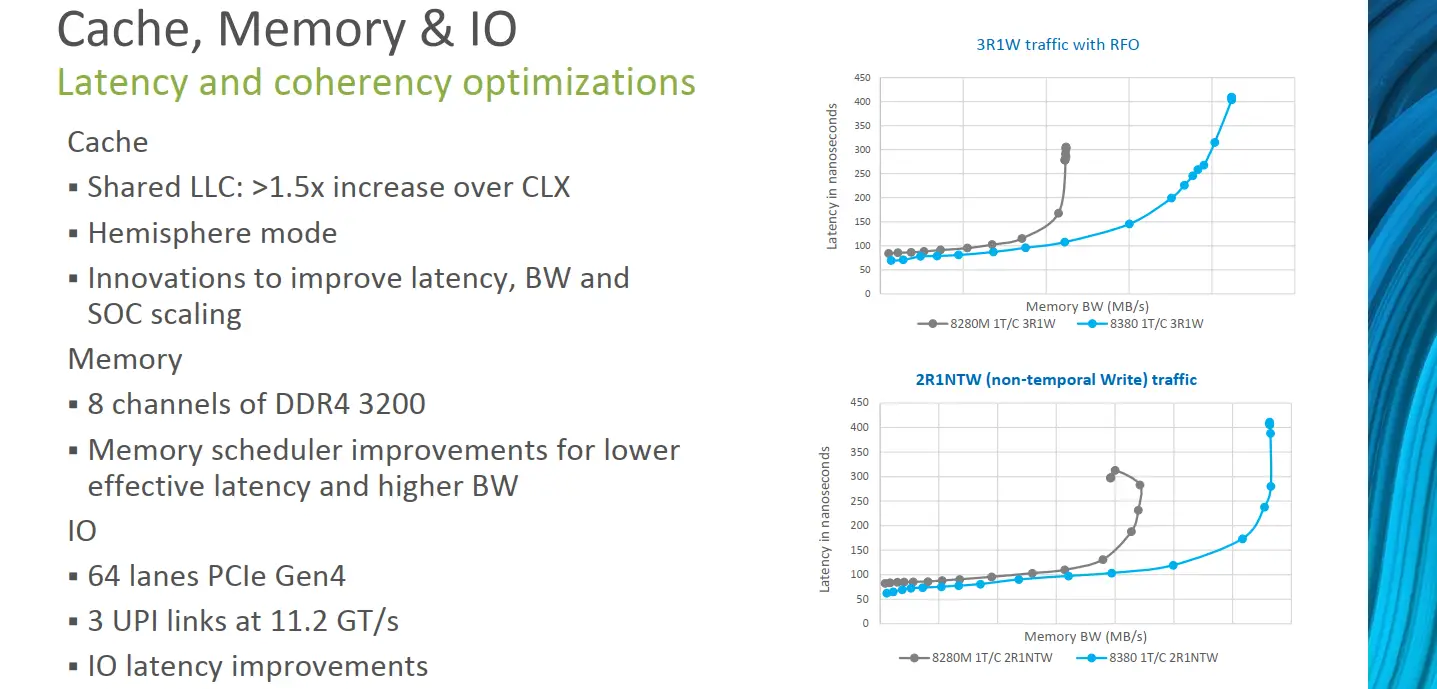
Ice Lake’s largest die supports up to 40 cores, 1.43x the core count over Skylake/Cascade Lake which topped out at 28 cores. This is a significant increase in core count compared to prior generations. In fact, a quick measurement based on the wafer photo reveals the 40-core die is roughly 628 mm², a sizable die for a first-generation 10nm server processor. The additional cores were introduced by adding a new row of cores to the mesh. The entire I/O subsystem on Ice Lake has also been enhanced. Two additional memory channels have been added, allowing for up to octa-channel memory support. For identical data rate DIMMs, this is roughly 33% higher bandwidth, however, Ice Lake also bumps the data rate to 3200 MT/s which can further increase the memory bandwidth depending on the DIMMs used. It’s worthy to note that with eight memory channels, Ice Lake has reached parity with both AMD and other Arm server chips. In tandem with the memory improvements, Ice Lake increases the PCIe lanes to 64 lanes or roughly 33% more lanes than Cascade Lake. Since Ice Lake now supports PCIe Gen4 which inherently doubles the bandwidth, the theoretical overall machine bandwidth is around 2.66x when fully saturated.
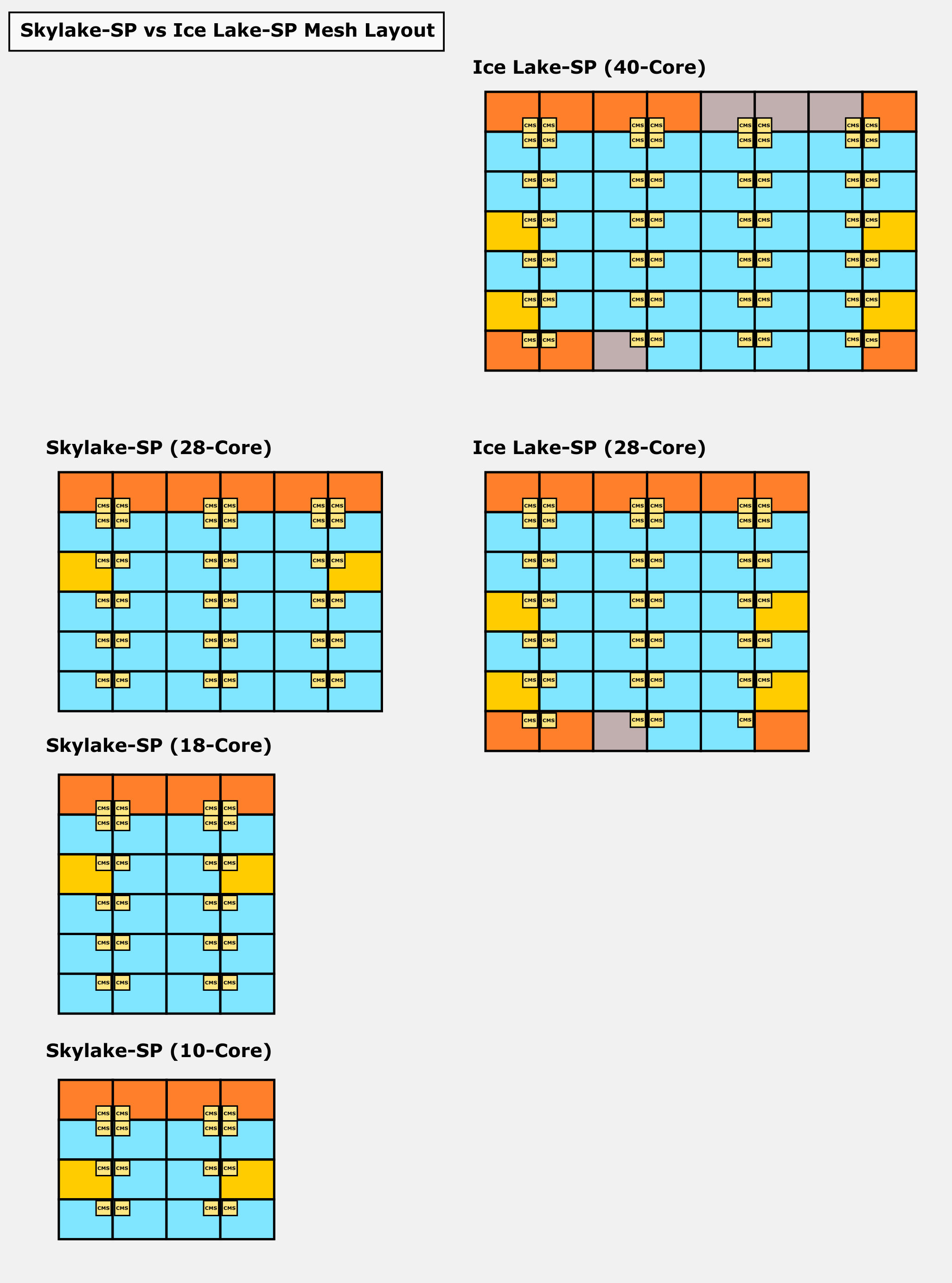
On Ice Lake, Intel broke down the memory controller tile into two tiles (shown in yellow in our diagram), so there are now four memory controllers, each housing two memory channels. This eases memory traffic across the mesh. Intel says the memory controllers have been enhanced with improved schedulers and larger queue sizes. It’s worth pointing out that Ice Lake SP introduces the Total Memory Encryption (TME) extension. The TME engine also sits in the memory controller themselves which is capable of encrypting the entire DRAM.
As with the memory controllers, the I/O tiles for the DMI and UPI links were also distributed across the south and north edges of the die on Ice Lake. Previously the entire SoC I/O situated at the north side of die in what Intel called the ‘North Cap’. A subtle but important change in the floorplan organization on Ice Lake is the distribution of interfaces themselves. Whereas on Skylake-SP, some of the I/O links shared the same tile and thus the same mesh stop (and bandwidth traffic), on Ice Lake every I/O link has its own tile and its own mesh stop. For example, the DMI interface sits on its own tile instead of sharing a tile with another PCIe x16 interface. Likewise, each of the UPI links also sits on its own, each having a dedicated mesh stop.
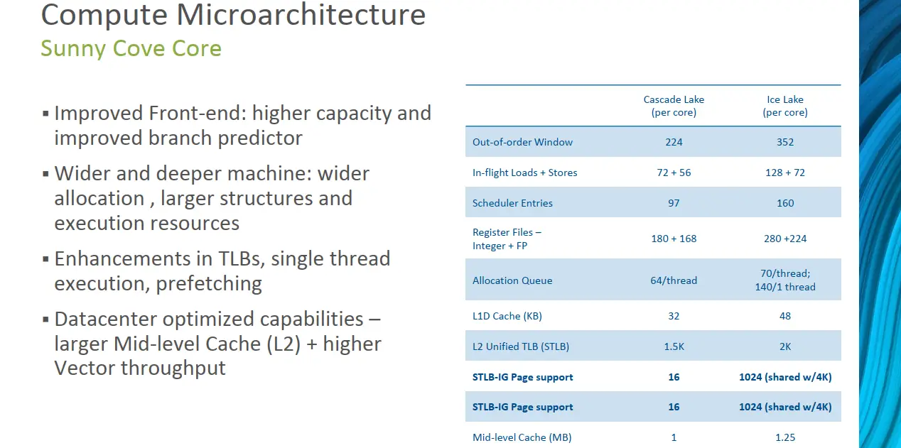
At the heart of the SoC are Sunny Cove cores. Intel says that on average they see around a 20% improvement in IPC. This is slightly higher than the 18% they reported earlier last year on pre-production silicon. The Sunny Cove implementation on Ice Lake SP is similar to that found in client chips, however, it does feature a slightly different cache hierarchy. Compared to Skylake-SP, both the medium-level cache and last-level cache have increased in capacity. With 1.5 MiB LLC per core, for the largest Ice Lake part with 40 cores, this works out to 60 MiB of LLC and another 53.75 MiB of MLC for a total cache capacity of just over 120 MiB.
| Cache Comparison | ||
|---|---|---|
| Microarchitecture | Cascade Lake | Ice Lake |
| L1I Cache | 32 KiB | 32 KiB |
| L1D Cache | 32 KiB | 48 KiB |
| MLC | 1 MiB | 1.28 MiB |
| LLC | 1.36 MiB | 1.5 MiB |
New Instructions
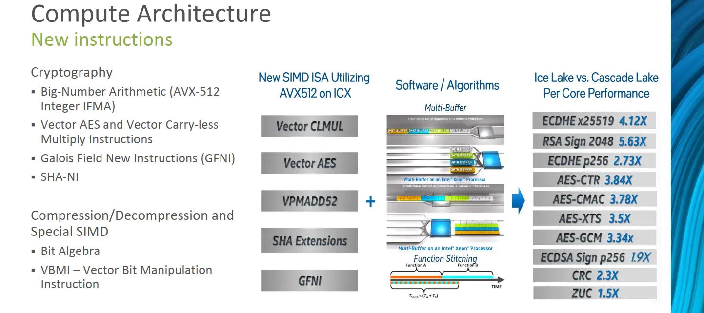
AVX-512 was first introduced in Skylake SP. Cascade Lake added a number of additional extensions for the manipulation of matrix multiplications for the acceleration of neural network algorithms. With Ice Lake, Intel is introducing a number of new extensions for the acceleration of cryptography and compression and decompression algorithms. Additionally, the VBMI/VBMI2 extensions are useful for various SIMD algorithms including those that rely heavily on moving bits around in the register. Not surprisingly, compared to Cascade Lake, Intel is reporting significant performance improvements for cryptography and compression algorithms that take advantage of the new extensions.
Beyond new instructions, Ice Lake also introduces two new security features. The first feature is Total Memory Encryption or TME which was initially announced in 2017. TME brings the ability to encrypt the entire memory address space. It can do this in two ways. The basic capability simply encrypts the full physical memory without modification to existing software by simply encrypting and decrypting the memory as it flows from/to the memory controllers. Alternatively, with software intervention, multiple keys can be utilized to encrypt subsets of memory by offering per-page encryption. Along with TME, On Ice Lake, Intel is also bringing the Software Guard Extension (SGX). Since servers typically have larger data sets, Intel says that up to 1 TiB is supported per secure enclave, although the exact size is determined per SKU.
AVX Frequencies
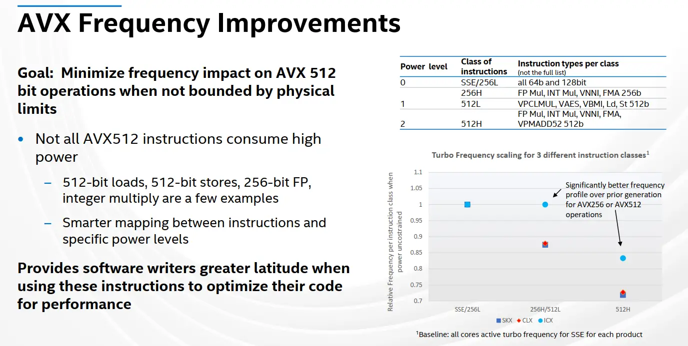
When AVX-512 first launched with Skylake-SP, it received some criticism from certain groups due to its severe downclocking. With the exception of certain SKUs, downclocking was actually not much of a problem, and utilizing AVX-512 produces superior performance even at lower frequencies. That said, not all AVX-512 instructions impact frequency the same way. Each SoC has three power levels for instructions – 0, 1, and 2. Power level 0 represents the usual power level and frequencies and is the power level for all the base instructions as well as 64b and 128b (SSE and 256 light) operations. The second power level groups the 256b heavy operations. Intel originally grouped AVX-512 instructions into AVX-512 light and heavy operations. Light AVX-512 operations fell into power level 1 and heavy AVX-512 operations fell into power level 2. Only AVX-512 heavy operation saw frequency downclocking. Simple operations, which are the majority of operations (those that do not involve floating-point or vector multiplication, fall into the AVX-512 light category. AVX-512 light actually executes at the AVX2 base and turbo frequencies which do not have any frequency reduction on recent chips.
On Ice Lake, Intel said they have revisited the issue and have made improvements to minimize the impact of frequency on AVX-512 workloads. AVX-512 instructions have been remapped in a better way to reflect the instructions and instruction stream’s overall power consumption. Intel says that when compared to prior generations (i.e., Skylake and Cascade Lake), customers can expect light AVX-512 operations as well as heavy 256b AVX operations to operate at frequencies very close to the normal (SSE-level) frequencies. In other words, there should be little to no downclocking for anything but heavy AVX-512 operations. Consequently, heavy AVX-512 operations should exhibit significantly less downclocking than prior generations.
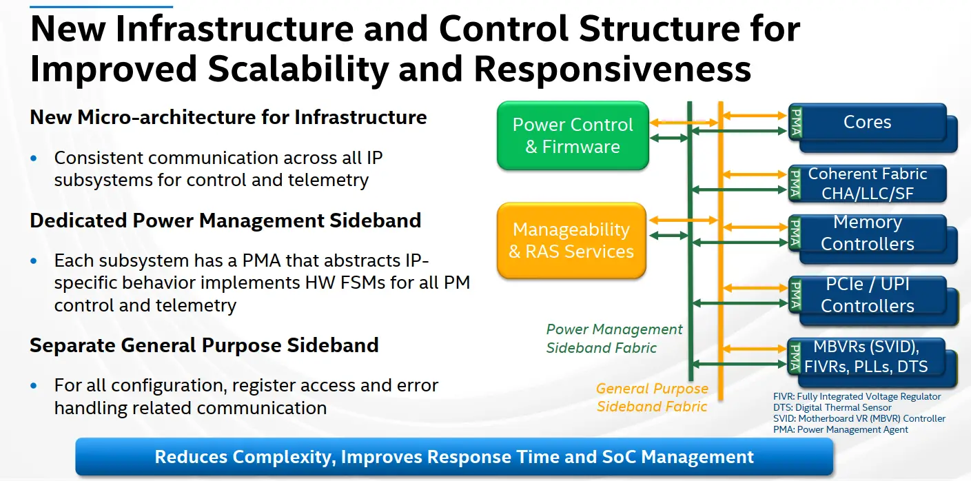
New Control Fabric
One of the other major areas of improvement on Ice Lake is the control fabric which has undergone significant overhauling. Intel says it has implemented a new microarchitecture to handle communication in a consistent way across all the connected IP subsystems on the chip for both telemetry and control. To that end, two new fabrics have been introduced – Power Management Sideband Fabric and a General Purpose Sideband Fabric.
The Power Management Sideband Fabric is a new fabric completely dedicated to power management. Shown in green on the slide below, the Power Unit (PUnit) now communicates with all the individual IPs through Power Management Agents (PMAs) which implements hardware FSMs for control and telemetry. The use of the PMA is designed such that the specific behavior of the IP can be abstracted from the rest of the system and is exposed through the PMA standard interface. Intel says the new fabric simplifies the SoC complexity, allows for better scalability, and improving responsiveness and SoC management.
Whitley
Ice Lake utilizes the Whitley platform. Up to eight DDR4-3200 (DPC) memory channels are supported on this platform along with 64 PCIe Gen4 lanes. Previously, Intel supported a maximum of six memory channels on both Skylake and Cascade Lake which proved to be quite a disadvantage when it comes to bandwidth-intensive workloads. Here, both Arm and AMD had the upper hand with their eight memory channels support. With six DDR4-2666 channels, Skylake can theoretically peak at 128 GB/s. Ice Lake bumps this to 204.8 GB/s, a 1.6x improvement.
Intel kept the number of UPI links the same as Skylake, however, they have increased the data rate. In Skylake, those links operated at a rate of 10.4 GT/s or 9.6 GT/s depending on SKU. In Ice Lake, Intel increased the peak data rate to 11.2 GT/s. In practice, this yields a modest improvement from 62.4 GB/s to 67.2 GB/s of peak bandwidth between two sockets in a 2-node platform. This is still significantly below the multi-socket bandwidth of their competition.
–
Spotted an error? Help us fix it! Simply select the problematic text and press Ctrl+Enter to notify us.
–