
TSMC 5-Nanometer Update
At the recent Arm TechCon TSMC gave an overview and status update of their current N7, N6, and the upcoming N5 process nodes.
N7
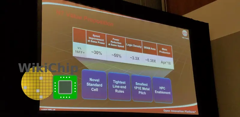
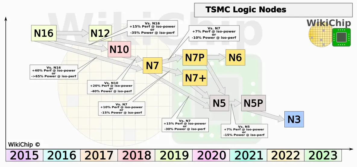
We have covered TSMC N7 process technology extensively over the last year. You can read our detailed coverage of the process from the VLSI Symposium here. TSMC gave a quick overview of their N7 once again. This is a process that ramped in April 2018 and has been in mass production for well over a year now. Compared to TSMC’s own 16FF+, N7 provides around 30% speed improvement at the same power or, alternatively, 55% power reduction at the same speed.
| TSMC Node Comparison | ||||
|---|---|---|---|---|
| Node | 16 nm | 10 nm | 7 nm | 7nm/10nm Δ |
| Gate | 90 nm | 66 nm | 57 nm | 0.86x |
| Min Metal | 64 nm | 42 nm | 40 nm | 0.95x |
The presenter mentioned a number of key innovations that went into N7 including a novel standard cell design which we do not believe were publically disclosed anywhere in detail.
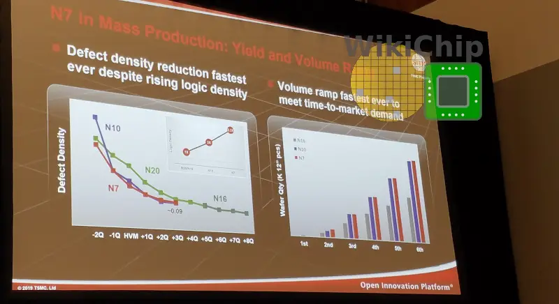
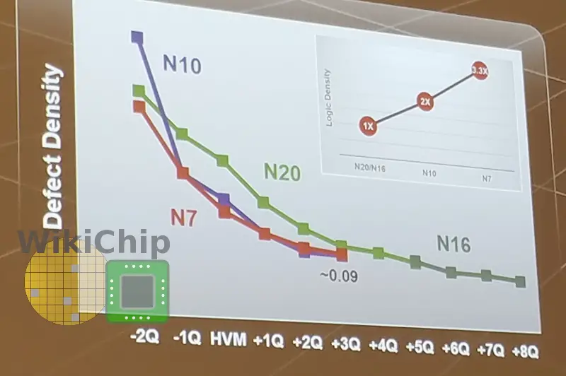
One of the things TSMC has reiterated is how fast they are able to ramp new nodes. Since its first FinFET node, N16, TSMC has been improving its volume ramp time each node. N7 is the company’s fastest ramp node in its history. The graph in the photo uses a baseline D0 of 0.09/cm². TSMC says it expects N6 to ramp just as fast and N5 is on a faster ramp trajectory.
N6
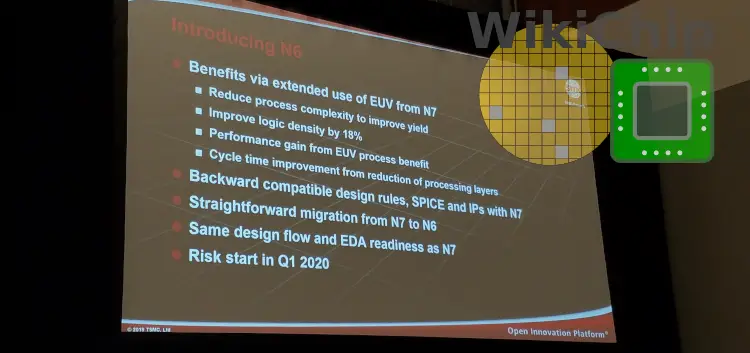
This year, TSMC ramped the N7+ node. This is its first EUV process which introduces EUV at a few critical layers for cost reduction and learning. Learning from N7+, next year TSMC will be introducing the N6 node. The reason for this new node is simple. N7+ is not IP-compatible with N7 making the transition more difficult. N6, on the other hand, allows for the same design rules as N7 thereby maintaining IP compatibility. N6 makes much more extensive use of EUV in order to improve yield and reduce cost by folding the number of masks. TMSC expects most N7 customers who are not looking to move to N5 right away to make the transition to N6 for the value proposition. The benefits TSMC highlighted for N6 is an 18% logic density improvement through the introduction of SDB, performance improvement from EUV lines, and significant cycle time improvement by reducing 2-4 masks down back to 1 mask.
TSMC expects N6 risk production to start in Q1 of next year with ramp planned by the end of 2020.
N5
N5 is TSMC’s next ‘full node’. TSMC expects N5 to ramp and reach high yield even faster than N7. A slight change from N7 is the fact that this node has been optimized upfront for both mobile and HPC. In the last few nodes, TSMC used to introduce a low-power mobile process first and then go back and optimize for HPC. With N5, TSMC says it has been optimizing the process for HPC right from the start. Compared to the standard N7 node, N5 provides around 15% higher performance at the iso-power or, alternatively, up to 30% power reduction at iso-performance. N5 also introduces new eLVT (extreme-LVT) devices for high-performance applications which can push the performance to as much as 25% higher at iso-power compared to N7.
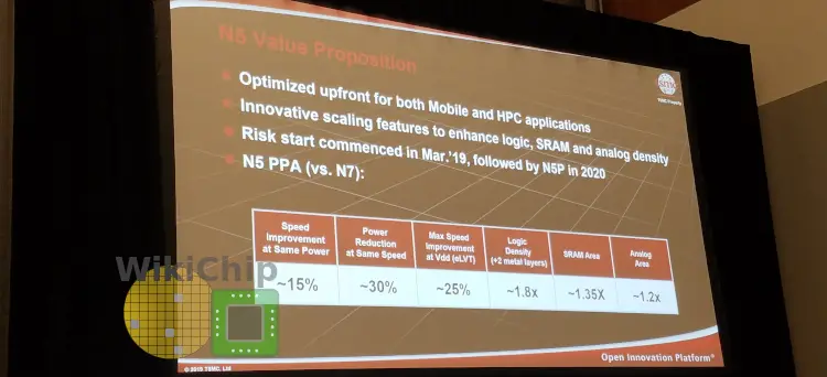
TSMC started risk production of N5 in March 2019. TSMC has said it has already taped out a number of products by lead customers and more tapeouts are expected in the next couple of quarters. TSMC expects to ramp N5 in the first half of next year – tentatively scheduled for Q1 2020.
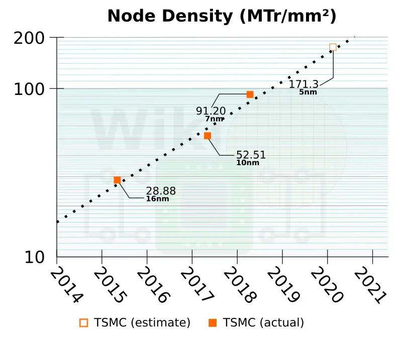
Compared to N7, N5 is said to provide a compaction ratio of 1.84x. TSMC said that one of the main features of N5 is the density improvement to analog devices which is something they have not really optimized in the last few nodes. To that end, it reports a 1.2x compaction of analog circuits. Based on what we have heard, WikiChip estimates the poly pitch to be around 48 nm along with a 30-nanometer metal pitch for an estimate transistor density of 171.3 MT/mm².
| Estimated Design Rules For 5 nm | |||
|---|---|---|---|
| 7 nm | 5 nm | ||
| CPP | 57 nm | 48 nm | |
| MMP | 40 nm | 30 nm | |
| Density | 91.2 MTr/mm² | 171.3 MTr/mm² | |
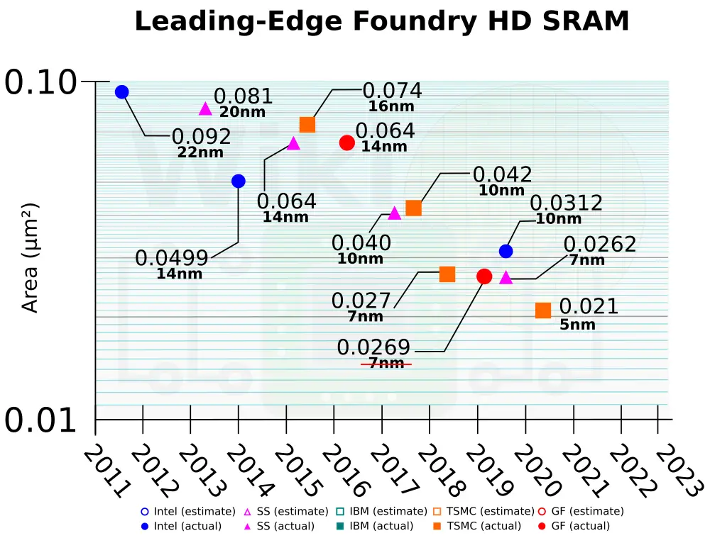
TSMC also disclosed its 5-nanometer 6T SRAM bitcell. The high-density N5 6T cell is 0.021µm², making it the densest production cell reported to date. Assuming a ballpark assist circuit overhead of around 30%, this works out to ~32 Mib/mm² of cache. This an increase of 30% from N7 which is around 24.7 Mib/mm².
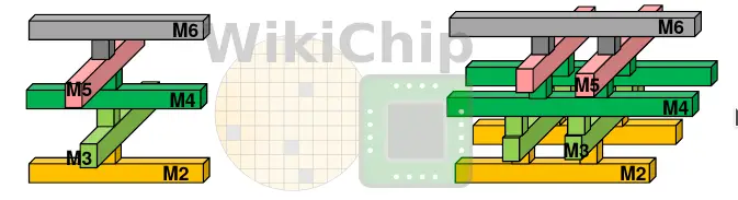
TSMC touched on a number of enhancements that were done at the N5 node. Since the wire resistance and via resistance continues to worsen at N5, for high-performance applications, N5 offers a slightly relaxed metal pitch and wider vias. Additionally, within a standard cell, the output can be optimized using custom via pillars (VP).
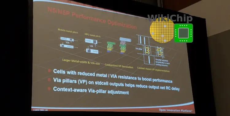
Via pillars are tightly-spaced identical via pairs placed in the main direction of the metal lines in a lattice structure. VPs help reduce the transistor, metal, and via resistance which helps reduce the RC delay through layer promotion (i.e., going up the metal stack) and via resistance reduction. The technique itself is not particularly new. Initial EDA-assisted support for VPs was introduced in N7, however, full VP enablement, including full VP generation and router capabilities are being fully rolled out with the new N5 HPC EDA design flows which has support for VPs in the P&R tools which can generate VPs based on the context around it in order to reduce the resistance and improve the performance.
N5P, N3
TSMC said that around Q2 2020 it will start the risk production of N5P. N5P is a planned performance-enhanced version of N5 and is planned to ramp one year after N5. Although the numbers are not concrete just yet, TSMC has said it expects N5P to deliver around a 7% performance improvement at iso-power or, alternatively, up to 15% reduction in power at iso-performance.
Looking a little further out, TSMC has started to talk a little about N3. N3 risk production is currently tentatively planned for early 2022 (but said it could be as early as late 2021). Depending on when risk production start, they expect it to ramp around the 2023 timeframe.
Derived WikiChip articles: 5 nm lithography process.
–
Spotted an error? Help us fix it! Simply select the problematic text and press Ctrl+Enter to notify us.
–