
Intel Looks to Advanced 3D Packaging For More-than-Moore to Supplement 10- and 7-Nanometer Nodes
Early last week Intel hosted an architecture day. The event was quite unique. It took place at the late Robert Noyce’s one-time home in Los Altos. There is a lot of history in that house. It was said that the room where the presentations were given was the original Intel boardroom. The day was packed with a mixture of technical presentations and 1-on-1 discussions with Intel executives, architects, and fellows. The much-welcomed event came after close to three years of radio silence concerning anything-10nm, architectures, and future roadmaps.
This article is part of a series that details Intel’s Architecture Day.
1. Advanced 3D Packaging For More-than-Moore to Supplement 10- and 7-Nanometer Nodes
2. Intel Discloses 10nm Sunny Cove and Core Roadmap, Teases Ice Lake Chips
Opening the day was Raja Koduri, SVP of the Core and Visual Computing Group, GM of edge computing solutions and chief architect at Intel Corporation. Koduri talk was extensive in both breadth and depth. In many ways, it was a breath of fresh air.
Architecture Era
Obligatory with every advanced technology talk is a mention of Moore’s Law. Koduri started with a discussion of historical trends – the megahertz era in the 80s and 90s and through the multi-core era in the 2000s and 2010s. “The key thing here is that we didn’t stop innovating because of the slope. We always found a way to innovate around that,” said Koduri. Koduri proposed that we are entering the architecture era, a time where innovation across the entire system architecture will be required to work around the limitations of physics.
A big part of keeping up the improvements to the system architecture remains the process technology. Intel generally has two process nodes. One process is optimized for compute performance while the other is optimized for I/O and SoC.
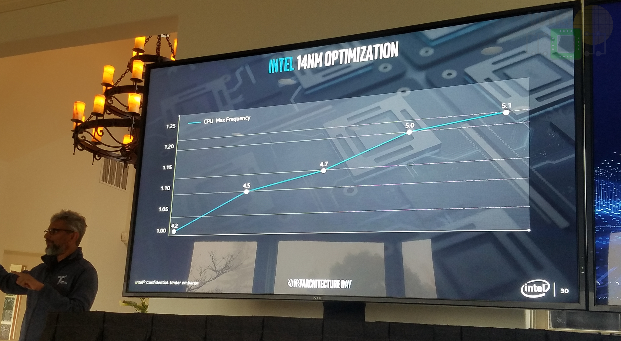
Intel’s lengthy stay at the 14-nanometer node due to their struggle with the 10-nanometer process has proven to be somewhat fruitful in a couple of unexpected ways. Through the various optimizations that were applied to their 14 nm process, they were able to extract a full-node worth of performance and power improvements. “We also learned that optimizations opportunities on each generation of transistors are tremendous,” said Koduri. It’s a lesson that Intel will be applying to their 10-nanometer node and all future nodes moving forward.
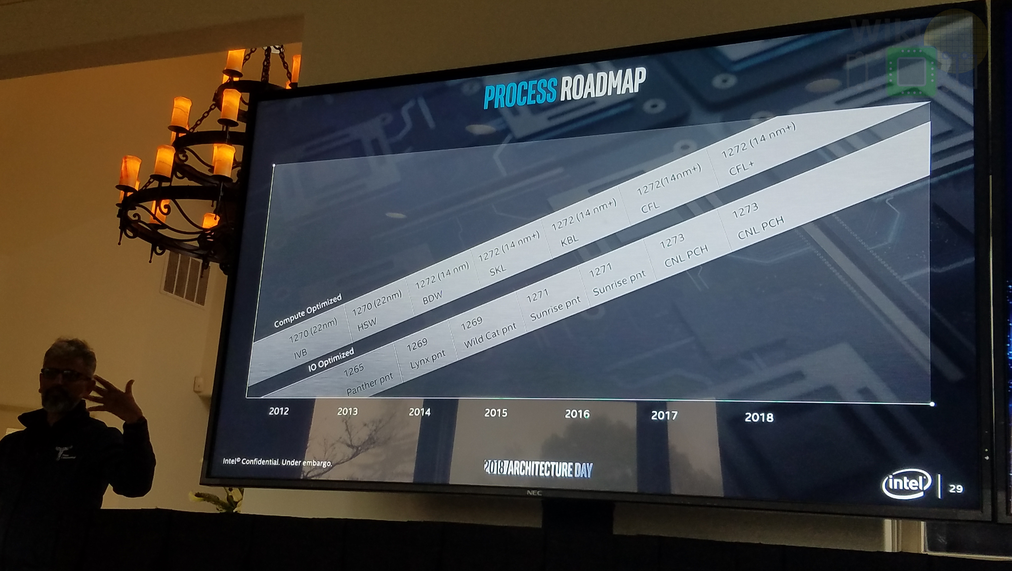
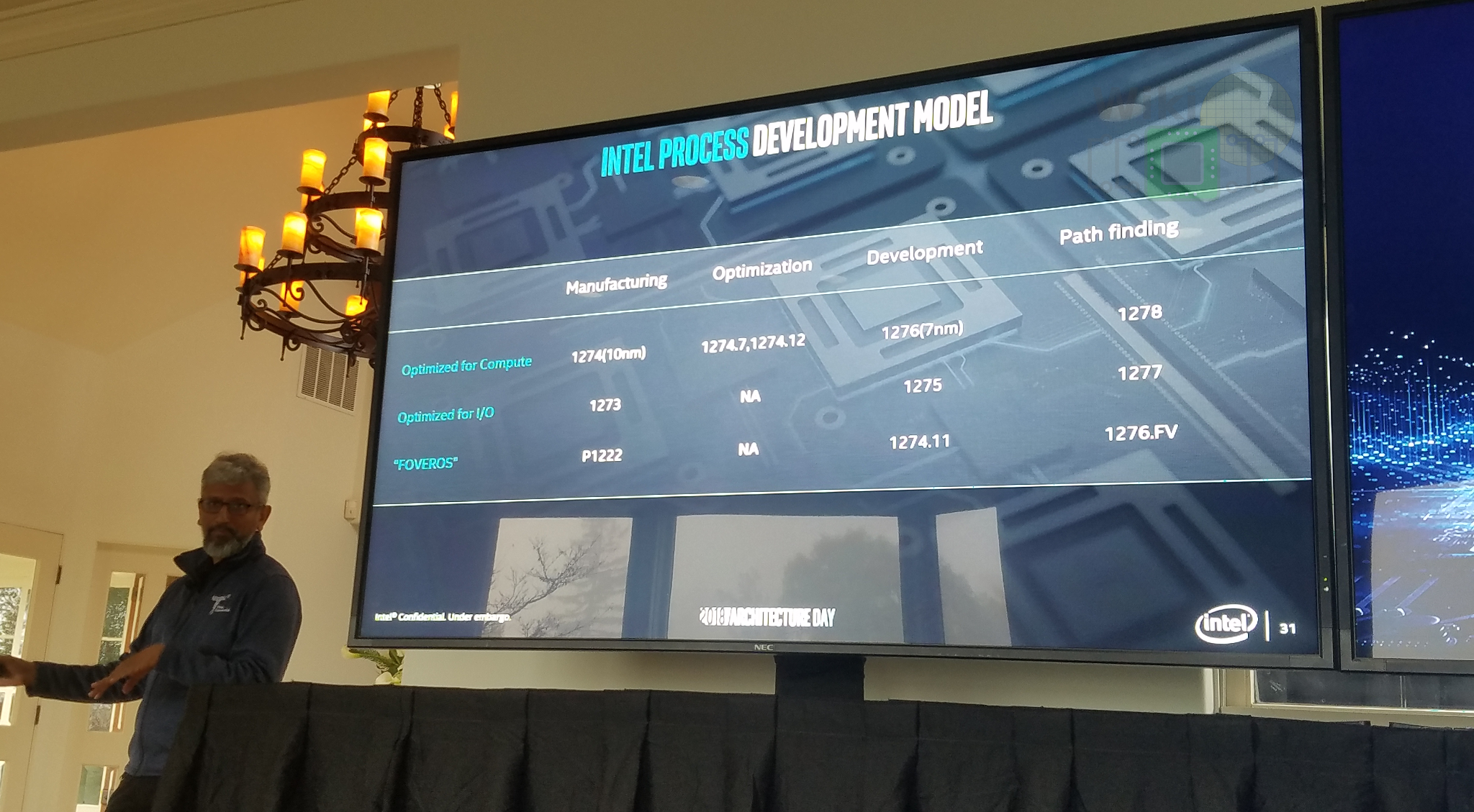
Moving to the current state of their process technology. Intel’s 10 nm node (P1274) is currently entering the manufacturing stage which will follow quickly by a set of two optimizations (P1274.7 and P1274.12) which are planned for the 10 nm and according to Koduri are expected to bring large improvements in performance and power. It’s worth noting that the ‘.7’ and ‘.12’ likely refers to the planned PDK introductory date (i.e. July and December). In the development stage is their 7-nanometer node (P1276) as well as the 10nm SoC variant (P1275). Looking a little further down the road, in path-finding stages is their 5-nanometer node (P1278) and the 7nm SoC variant (P1277). Beyond acknowledging the existence of those future process technologies, Intel isn’t ready to talk specs just yet. This isn’t too surprising. Process technology details are almost always kept secret until released due to competitive reasons.
If you are having a hard time keeping track of all those codenames, here’s a quick simple rundown. The first one/two digits refer to the wafer size. For example, the 80486 made on 0.8-micron was called “P650″ because it used 6” wafers (150 mm), likewise, Coffee Lake is made on 14 nm internally called “P1272″ which uses 12” (300 mm) wafers. The last two digits refer to the process and those are simply auto-incremented each node – dating back to the original 8086. For example, Intel’s 1-micron tech was 48/49, 0.8-micron was 50/51, all the way to today with 14nm being 72/73. Even numbers refer to their performance-optimized nodes while odd numbers refer to their I/O and SoC optimized nodes. Generally, the I/O-optimized process trails the other process by a couple of years. For example, Haswell (22 nm) is on P1270 while 200-series Sunrise Point chipsets (also 22nm) are on P1271. Today, Skylake (14 nm) is made on P1272 while the 300-series Cannon Point chipsets (also 14 nm) are made on P1273.

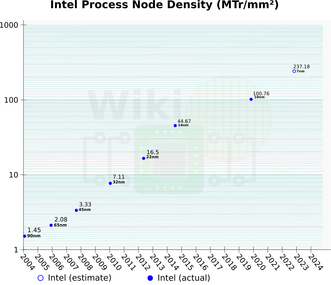
Intel’s 10-nanometer node high-density standard library cells have a density of 100.8 MTr/mm² based on their density metric. On April 26, 2018, during Intel’s Q1 earnings call, Brian Krzanich disclosed that Intel’s 7-nanometer node has a compaction number of 2.4x. We estimate that puts them at around 237 MTr/mm² for their seven nanometers.
The Case For Advanced Packaging
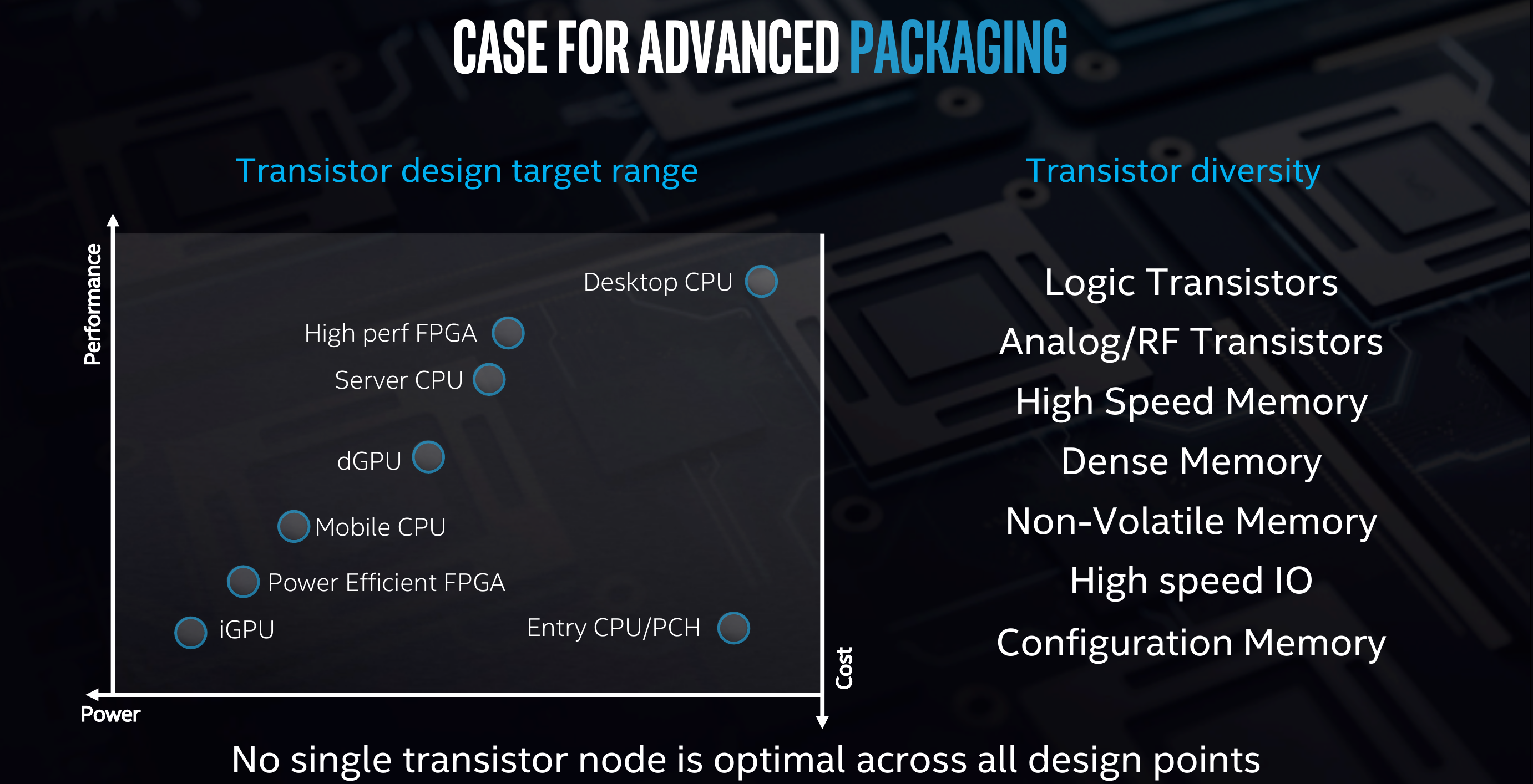
One of the things Koduri touched on is the notion of transistor diversity. Attempting to enter different markets means designing products that vary greatly in the type of transistor that’s optimal for that segment. For example, the transistors used for high-performance desktop CPUs and FPGAs have very different performance/power design points compared to the transistors used to design integrated GPUs and power-efficient FPGAs. There is also a cost factor involved. In essence, not only will one transistor not fit all, but the newest transistor isn’t even necessarily the best one for the job. This is a very important point not often discussed. Process technologies are often presented as a homogeneous set of transistors. Companies, including Intel, are certainly guilty of this by only boasting about their high-density standard library cells and high-density SRAM. Of course, marketing and PR is involved here but that does tend to hide much of the complexity. It’s worth noting that this year Intel did talk about their 10 nm libraries at IEDM and we will have coverage of that in an upcoming article.

Introducing Foveros
The growing diversity of transistors that is brought about by the increased diversity of integrated circuits (e.g., PCH, CPU, GPU, NPU, FPGAs, RF, memory) means it’s more desirable than ever to piece together larger ICs out of smaller dies – each purpose-built using the best process for the job. We have seen this with products such as Intel’s Stratix FPGA and Kaby Lake G. AMD’s upcoming Zen 2 also incorporates an I/O die fabricated on a different process than the compute dies, leveraging a mature process for the I/O and taking advantage of the performance and power advantages of a leading edge node for compute.
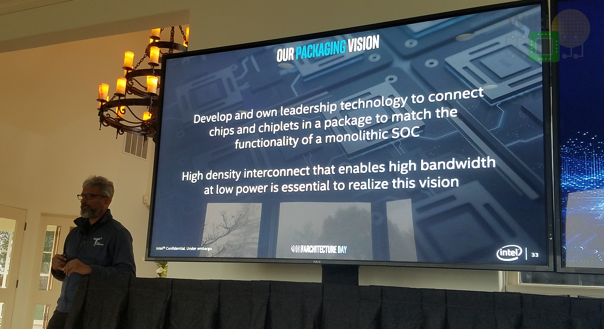
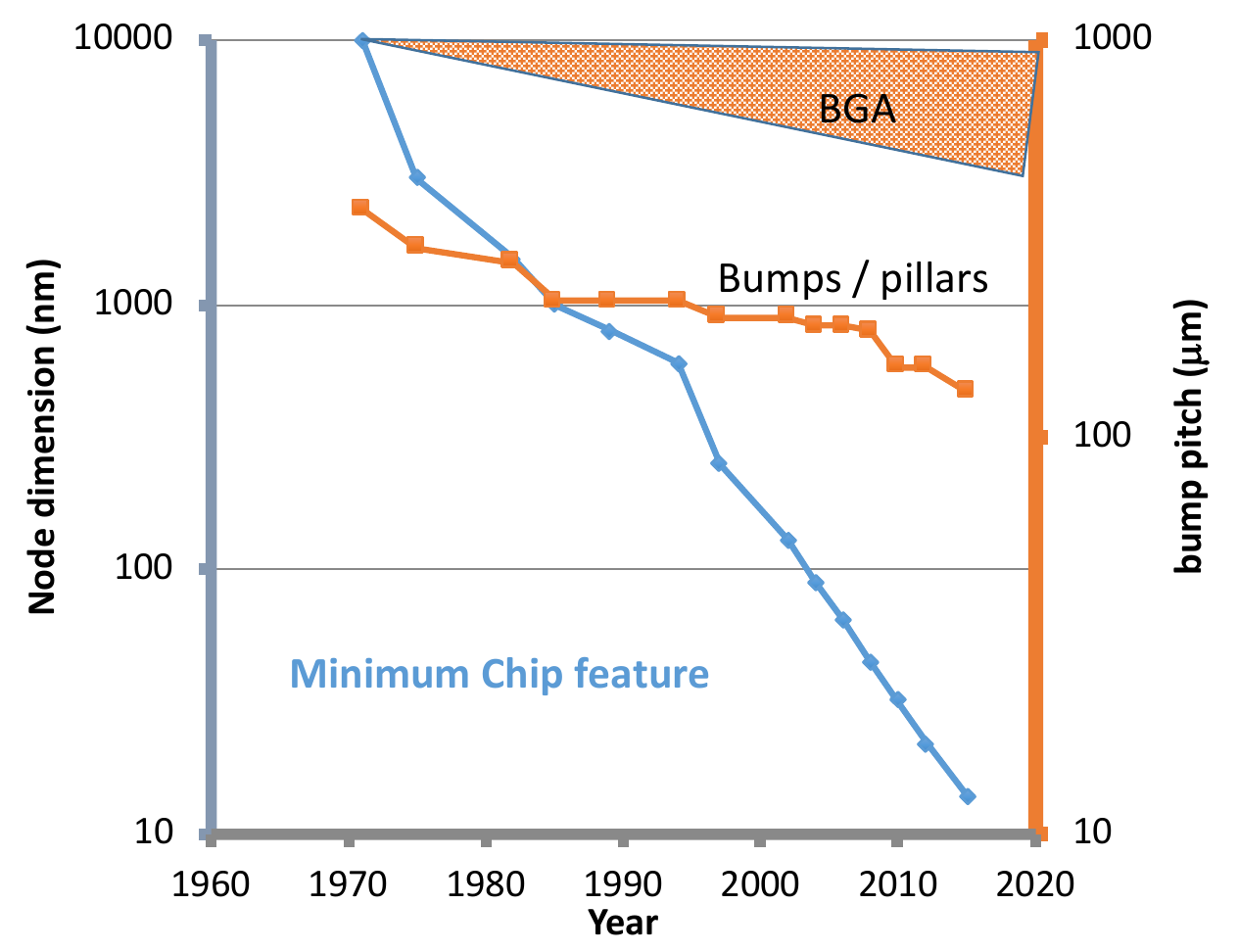
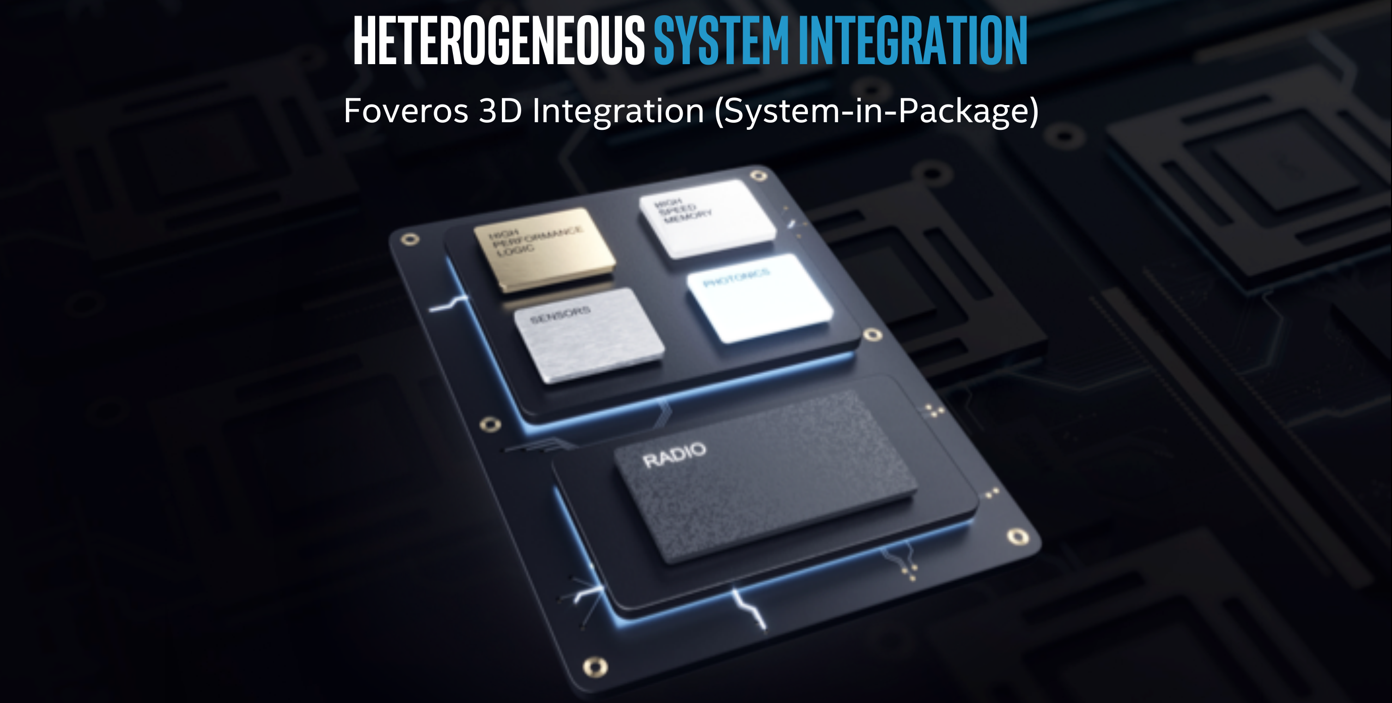
All of this brings us to Foveros (φοβεÏός in Greek meaning awesome, fearful, and terrifying) – Intel’s solution to the problem of developing independent chiplets on their own optimal processes and then interconnecting them in a single package to match the functionality of a monolithic SoC. As you can imagine, this is much easier said than done. The industry has been working on 3D packaging for decades now. For example, an early research project from Intel is Polaris, one of the projects as part of their Tera-Scale Computing Research Program in the early 2000s. Polaris stacked a large SRAM die on top of the processor chip in order to achieve a very high memory bandwidth. A major packaging challenge historically has been the bumps/pillar and interconnect among many other. Data movement across dies can take up a large portion of the total package available power. In fact, the fine pitch interconnects from die-to-package are largely limited by mass reflow which has prevented them from scaling much in recent nodes. A great property of solder bumps is that there is so much substance there that when it flows, it’s able to accommodate all the non-uniformities of the die and the package.
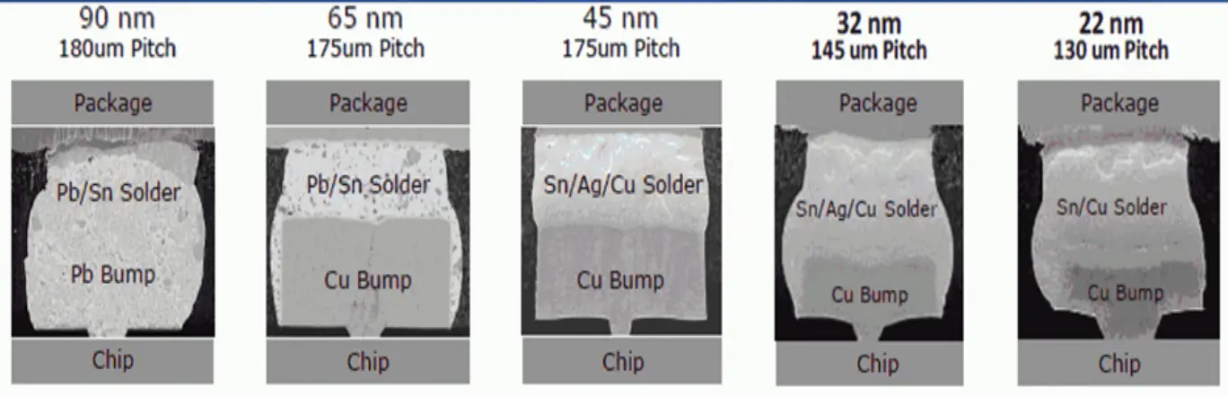
This is where the true benefits of Si interposers (2.5D) and die stacking (3D) are realized. Compared to a standard package with a bump pitch of around 110-micron and yields around 1.7 pJ/bit, Intel’s side-by-side EMIB (2.5D) solution is around 45-micron pitch and at around one-sixth the power per bit transferred at 0.30 pJ/bit. The power efficiency comes from traces never leaving the silicon to the actual organic substrate which means the wires can be smaller. Foveros, on the other hand, goes one step further with 3D die stacking. Foveros goes down to 36-micron bump pitch with a bump density of 828/mm² and half the power of EMIB with around 0.15 pJ/bit. That’s a significant reduction in the amount of energy required to move data around. At a fixed power envelope, the less energy spent per bit, the more bits can be transferred, or alternatively, that energy can be spent on other resources.

Anatomy of Foveros
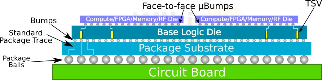
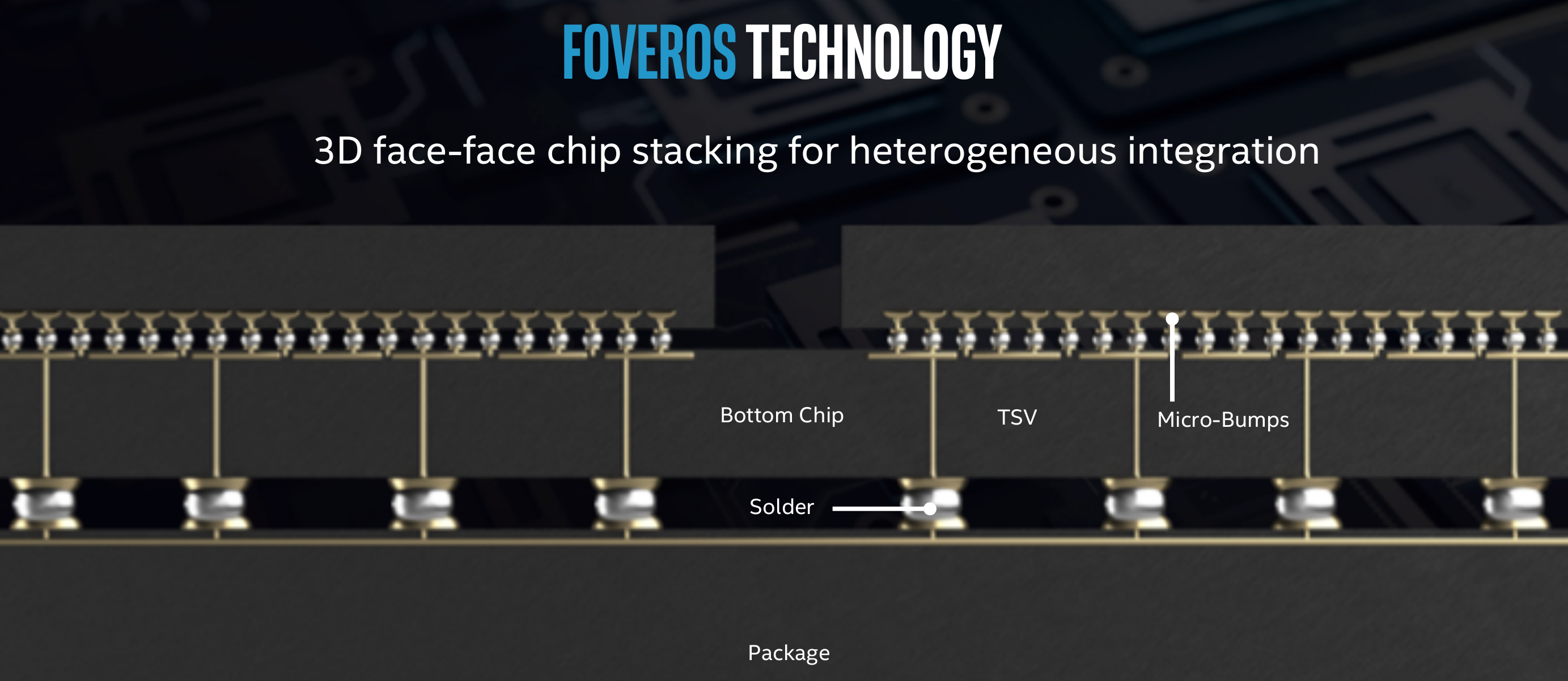
Foveros is an advanced 3D face-to-face die stacking packaging process technology. The technology is designed to incorporate two or more dies assembled together. It comprises a base logic die on top of which sit additional active components such as another logic die, memory, FPGA, or even analog/RF.
The key feature of Foveros is the face-to-face (F2F) chip-on-chip bonding through extremely fin-pitched, 36-micron, microbumps (mostly likely copper pillars). Intel hasn’t delved into the process flow, although we do expect a paper to be presented sometimes in the future. F2F flow is somewhat fairly straightforward. Bumping is done to the base and top dies followed by backgrinding and then singulation. We have confirmed the thinning part. They likely use TCB-NCP for the final assembly, but this is pure speculation. The main benefits of F2F are the interconnect density scaling and lower wire parasitics which is important of high-performance applications like those used by Intel.
It’s worth noting that Intel isn’t actually first with such technology. 3D designs are in use in various niche markets, and their benefits are proven. Foveros is aimed at a very broad set of applications targeting very advanced electrical characteristics and interconnects. There is the flexibility aspect of the technology as well. Foveros is designed for logic-on-logic beyond memory as well as multiple dies on top of a base logic. Needless to say, Foveros is a VERY complex packaging technology. Intel says they set out to design a process for connecting chiplets together in a way that matches the functionality and electrical characteristics of a monolithic SoC and Foveros seems to do just that.
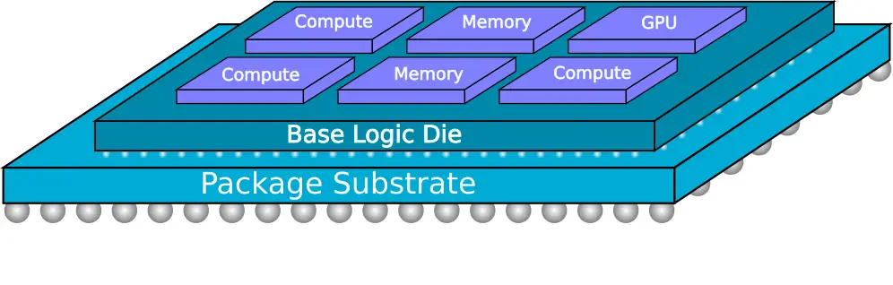
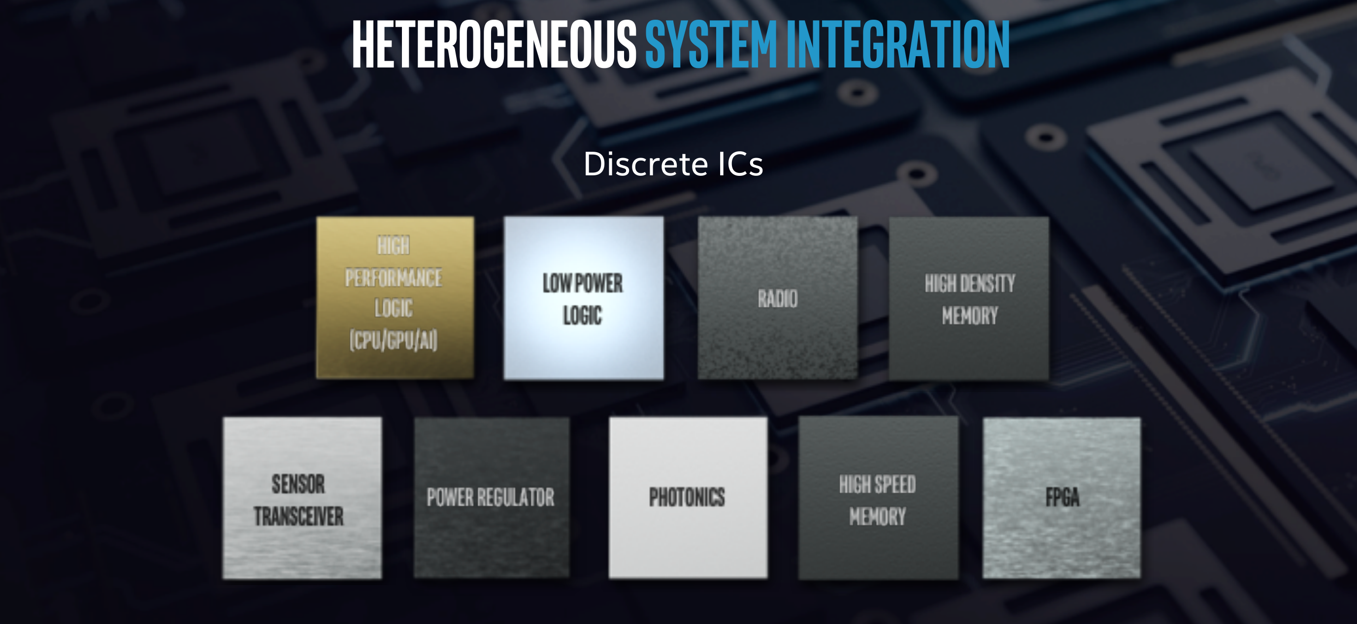
They listed some examples of the discrete ICs that could be mixed and matched.
Ready for Prime Time
3D packaging comes with a whole set of challenges. Raja Koduri mentioned three of them: thermals, power delivery, and yield. A major consequence of stacking multiple active dies on top of one another is the significant increase in heat density. Power delivery and power rails routing between the top and bottom logic dies is the second issue. Finally, he named known good dies (KGD) detection as the third challenge. Detecting of known good dies prior to assembly is a big issue in order to prevent throwing away a whole package due to just one bad die, making the manufacturing process cost prohibitive. Beyond those issues, there is the EDA tools aspect and challenges pertaining to accurate modeling and simulation of the package and the dies behavior. Intel says they have been working on solving those challenges for more than twenty years. “We feel we finally figured out how to make this a high-volume manufacturable product,” Koduri said.
Beyond solving the packaging-related challenges, the timing itself is a bit suspicious. Intel’s long delays due to their struggle with the ten-nanometer node meant competing foundries have managed to catch up, at least on some criteria. On top of that, process nodes no longer offer the same performance and power benefits it once did. And then there is the cost. Manufacturing large dies are getting more and more expensive. And let’s not forget the nasty speculative execution related vulnerabilities which resulted in a performance hit once patched. What Intel might really need is an edge. A disruptive technology. Foveros could be this technology.
–
Spotted an error? Help us fix it! Simply select the problematic text and press Ctrl+Enter to notify us.
–