
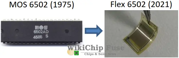
Reincarnating The 6502 Using Flexible TFT Tech For IoT
Despite being nearly 47 years old, the MOS Tech 6502 – or its low-power direct equivalents – is still being manufactured and is widely used in consumer products such as toys, automotive, and appliances as well as in embedded and industrial applications. It would seem that interest in this chip isn’t dying out any time soon. Due to its simple design and the large existing repository of knowledge and code, this chip could find new uses in the emerging world of IoT and ubiquitous computing.
At the recent 2022 International Solid-State Circuits Conference (ISSCC), a team of researchers from the University of KU Leuven in collaboration with imec and PragmatIC Semi presented the world’s fastest TFT-based processor, the Flex6502.
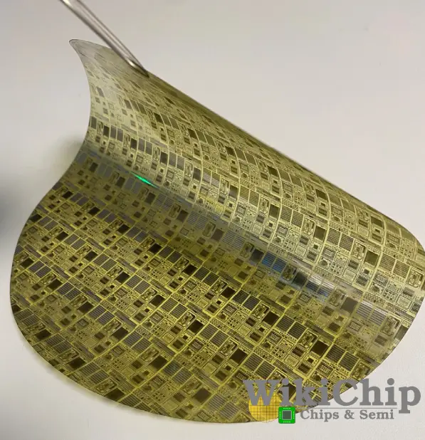
Highly integrated systems manufactured using Thin-film technology on a flexible substrate are an attractive area of research due to the relatively lower cost, mass production capabilities, as well as the unique use cases they can offer such as enabling seamless integration of electronic circuits on everyday objects. While your typical silicon die thickness is in the 100s of microns, thin-film can be less than 20 microns making them highly bendable. There are, however, various other tradeoffs when dealing with plastic electronics such as lower performance due to the mobility of the material and device dimensions. For the Flex6502, the researchers utilized PragmatIC Semiconductor’s 0.8 μm FlexLogIC fabrication line.
![]()
FlexLogIC technology is a 0.8-micron process with an actual channel length of around 800 nm featuring only four metal layers. It is an n-type metal-oxide TFT technology and is based on Indium Gallium Zinc Oxide (IGZO) manufactured on an 8″ polyimide wafer less than 30 μm thick. Coincidently, There are a number of major barriers preventing mass production of large integrated systems not too dissimilar from the challenges engineers faced during the 1970s when the 6502 was first made. FlexLogIC fab suffers from high power consumption, poor noise margin, and large process variation. Beyond being a monotype process, they also only offer a single Vt device. Furthermore, no fully verified design follow is currently offered by foundries.
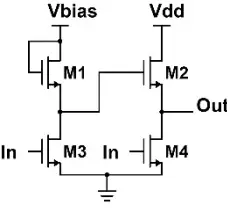
For the Flex6502, the designers allocated two metal layers for the gate and source/drain and the two remaining layers for routing. Addressing the design restrictions of IGZO TFT technology, Flex6502 utilizes Pseudo-CMOS, a technique first described by the University of Tokyo in the 2010 IEEE Transactions on Electron Devices. Invented specifically for working with the limitations of TFT technology, it claims to offer comparable performance with the complementary type and dual-VT designs while utilizing a single Vt monotype design. Additionally, it has the benefit of offering post-fabrication tunability, allowing it to compensate for process variants. Pseudo-CMOS does consume a larger amount of area compared to some of the other TFT-compatible logic such as resistive-load.
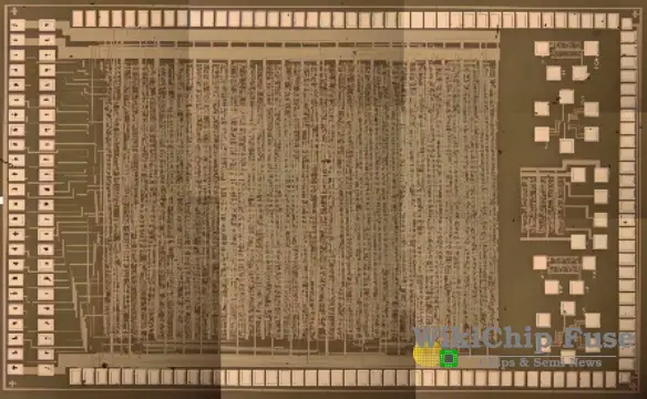
Addressing the lack of a fully verified physical implementation flow for TFT in terms of power and timing, the team implemented a full design flow for TFT. The Flex6502 relies on the ag_6502 FreeCore available online with some further optimizations such as the elimination of decimal mode due to lack of usage in order to reduce its size. The team initially relied on a standard foundry standard-cell library comprising 560 cells as their starting point in order to synthesize their core. Redundant cells were eliminated and less commonly-used cells were replaced with alternative equivalent implementations. Finally, the remaining cells (60 cells in total) were optimized for N-type monotype single Vt TFT technology. This produced a 23-cell library. The researchers then produced a schematic and layout design for the cells for TFT technology using a NOR-based design with a maximum of 2 TFT pull-downs which was used for the fabrication of the chip.
All in all, the Flex6502 was synthesized and fabricated as 1718 standard cells integrating 16,393 TFTs in a 24.9 mm² area. Roughly 18.6% of the design is inverters, 17.4% NAND2, 13.5% NOR2, and 7.1% AOI22. All other cells make up the remaining 43%. The chip was validated and tested using an FPGA which emulated the memory, UART communication, and clock generation. The chip achieved a maximum operating speed of 71.4 kHz (at Vdd=3V/Vbias=6V) while consuming a maximum of 134.91 mW. Likewise, the chip can run as low as 10 kHz at 2V while consuming just 11.6 mW.
–
Spotted an error? Help us fix it! Simply select the problematic text and press Ctrl+Enter to notify us.
–