
GlobalFoundries, Arm Demonstrate High-Density 3D Stacked Mesh Interconnect for HPC Applications
Recently, Arm announced the tape-out of an interesting test chip. But before delving into the chip itself, it’s worth highlighting a number of advanced technologies that are reaching an intersection.
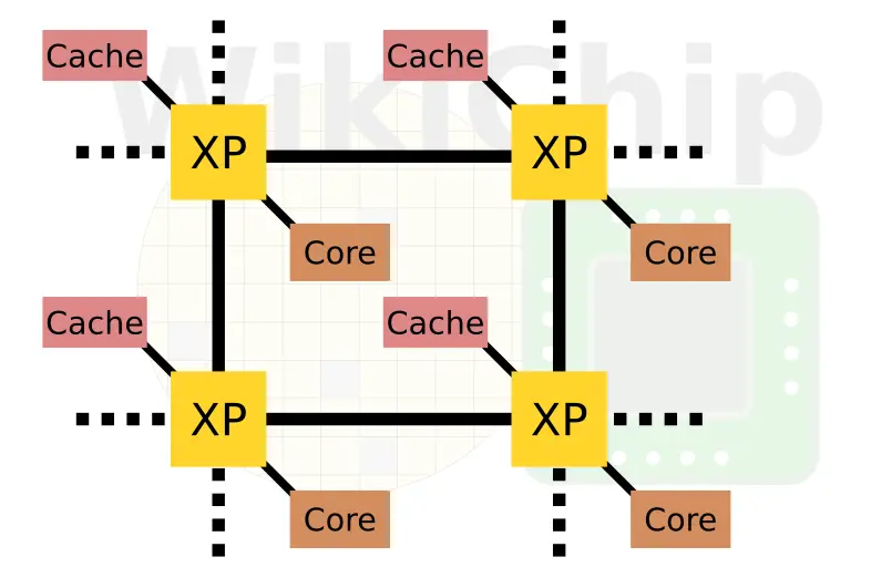
In 2016, Arm announced the coherent mesh network 600 (CMN-600), a shift to a mesh interconnect from the older cache coherent network 500 (CCN-500). The CMN-600 architecture comprises a grid of network routers known as crosspoints (XP). Each XP is extended to other XPs in a 2D mesh. Attached to each router is up to two AMBA CHI (Coherent Hub Interface) compliant devices. In the case of something like Arm’s recently announced Neoverse N1, it’s a slice of system cache and a core.
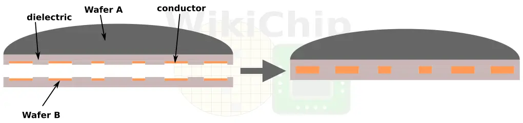
In an effort to aid traditional silicon scaling, 3D IC has emerged as a viable method of scaling beyond the planar surface. The current methods of linking together dies utilize mechanisms such as micro-bumps which are challenging to work with. It’s a complex process with warpage, stress, thermal, and performance issues that are not scaling well. But the industry needs to scale. And by a lot. This is where hybrid bonding comes in. Hybrid bonding (also known to some of our readers as DBI) has been a long-term goal for the semiconductor industry. Hybrid bonding is a promising alternative to traditional thermocompression bonding (TBC) 3-dimensional integrated circuit technology. It’s a highly-align-accurate highly precise, bonding technology that can enable direct Cu-to-Cu and oxide-to-oxide bonding interfacing with sub-10-micron pitch bonding.
The last piece of that is coming together is emerging memory technologies such as ReRAM and MRAM which could serve as highly dense on-die non-volatile storage or slower caches.
Trishul Test Chip
All the technologies above finally lead us to Trishul, Arm’s first high-density 3D test chip. Recently, GF taped-out the test chip which it expects to enable the next-generation high-performance computing applications such as AI with a higher level of integration – particularly in the 3rd dimension.
The test chip, which represents the ongoing collaboration between GlobalFoundries and Arm, was fabricated on GlobalFoundries 12-nanometer (12LP) process. The chip integrates Arm’s CMN-600 mesh interconnect using 4 routers. But unlike traditional chips, on this test chip, there are two routers connected in 2D on one die and two more routers connected in 2D on a separate die. The two dies are then stacked together and each router is also connected to the router on the opposite die. In other words, this chip features the first 3D mesh interconnect implementation of the CMN-600.
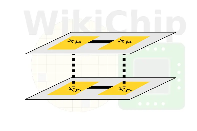
The two dies are interfaced using hybrid bonding with sub-10 um bond pitches – a massive improvement over current face-to-face micro-bump densities. In theory, this could allow GF to scale to millions of 3D connections per mm². On this test chip they are not quite there, but it is significantly denser than current packaging technologies. The chip features about 3000 3D connections between each router for a total of over 10,000 3D connections across the entire chip.
The dense 3D connections enable lower capacitance and lower latency. They can be used to minimize routing paths. In conjunction with some of the emerging technologies such as ReRAM and MRAM, new architectural improvements could come from storing certain types of data directly above the processing elements.
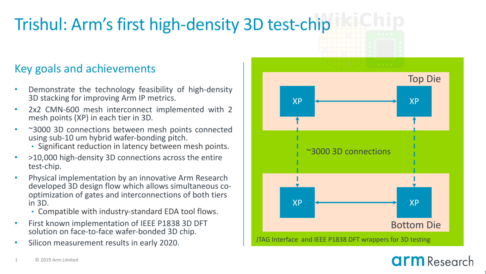
Beyond the technological capabilities of the chip, this test chip is also the first known implementation of IEEE P1838 3D DFT, an IEEE design-for-test (DfT) architecture standard that allows sending test control and data signals up and down the die stack for efficient testing.
GF expects 10um and sub-10um pitch interconnects to be available using the 3D connections. Looking a little bit out, GF says that their hybrid bonding technology is capable of up to 1 million 3D connections per mm2. This requires 1um pitch bonding which can be done as long as the extreme alignment accuracy can be achieved by commercially available wafer-to-wafer bonding tool.
Silicon measurement results for the test chip will be available in early 2020. GlobalFoundries expects 12LP hybrid bonding to reach qualification in 2020, with manufacturing readiness in 2021.
–
Spotted an error? Help us fix it! Simply select the problematic text and press Ctrl+Enter to notify us.
–