
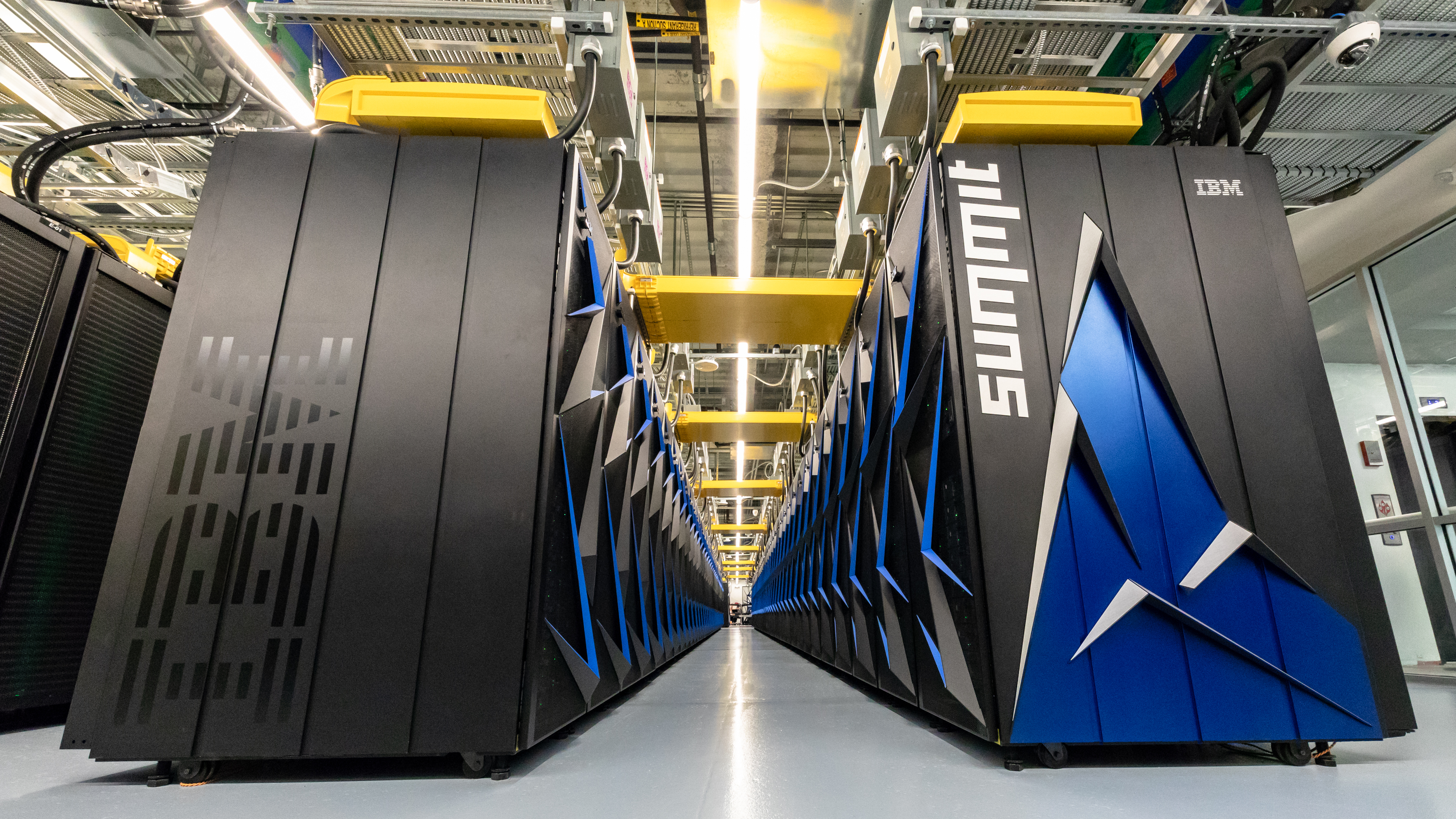
ORNL’s 200-petaFLOPS Summit Supercomputer Has Arrived, To Become World’s Fastest
Last Friday, the Department of Energy Summit supercomputer was officially unveiled by Oak Ridge National Laboratory (ORNL). Summit is a result of roughly a 200-million dollars investment as part of the CORAL procurement program and a multi-year effort by ORNL, IBM, and Nvidia. With 200 petaFLOPS peak performance and 3.3 ExaOPS for AI workloads, the Summit supercomputer is expected to become the world’s fastest – a spot held by China for the last half-decade. The TOP500 crowning will officially take place in Frankfurt, Germany (June 24-28). As long as there are no surprises from China, Summit is expected to dethrone the Sunway TaihuLight as the world’s fastest.
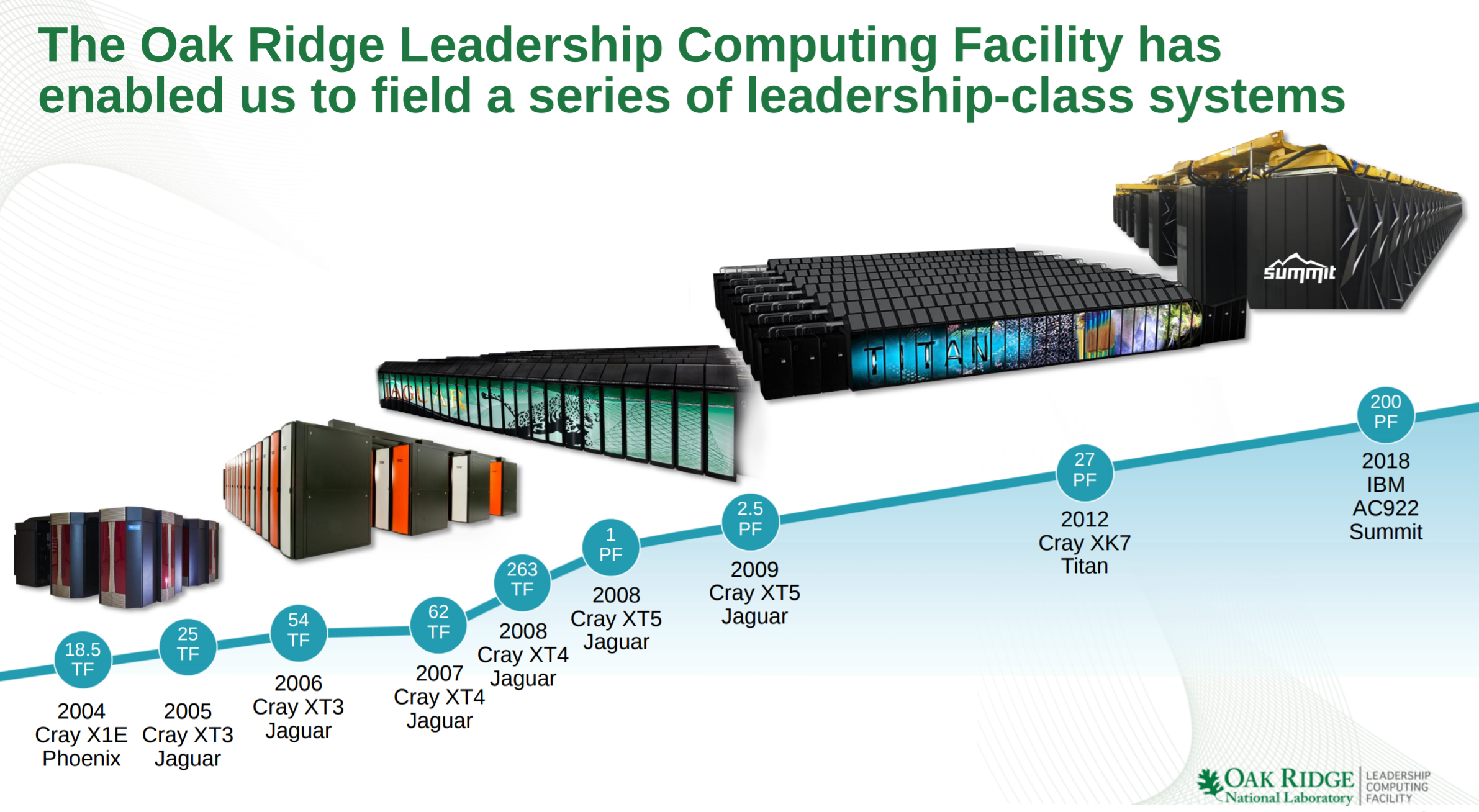
Summit is replacing its predecessor, Titan, which had a theoretical peak performance of 27 petaFLOPS – about a tenth of the compute power. Whereas Titan featured 18,688 nodes of AMD Opteron and Nvidia Kepler GPUs, Summit is using much denser 4,608 nodes of IBM POWER9 and Nvidia Volta GPUs. The close to 10x in performance is reached while increasing the power consumption by only 1.4x to 13 MW from 9 MW in Titan. It’s worth pointing out that the goal of Summit was not to reach some specific compute power but to achieve 5-10x improvement in real-world application performance.
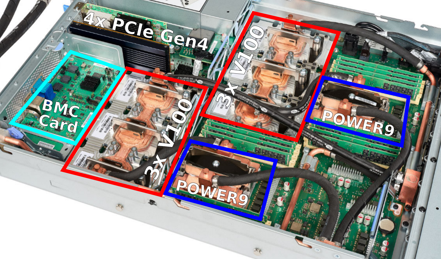
Compute Node
The basic compute node is the Power Systems AC922 (Accelerated Computing), formerly codename Witherspoon. The AC922 comes in a 19-inch 2U rack-mount case.
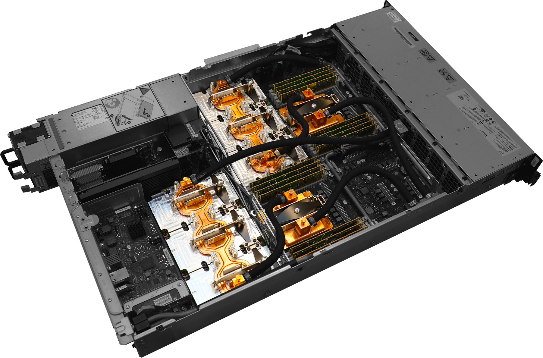
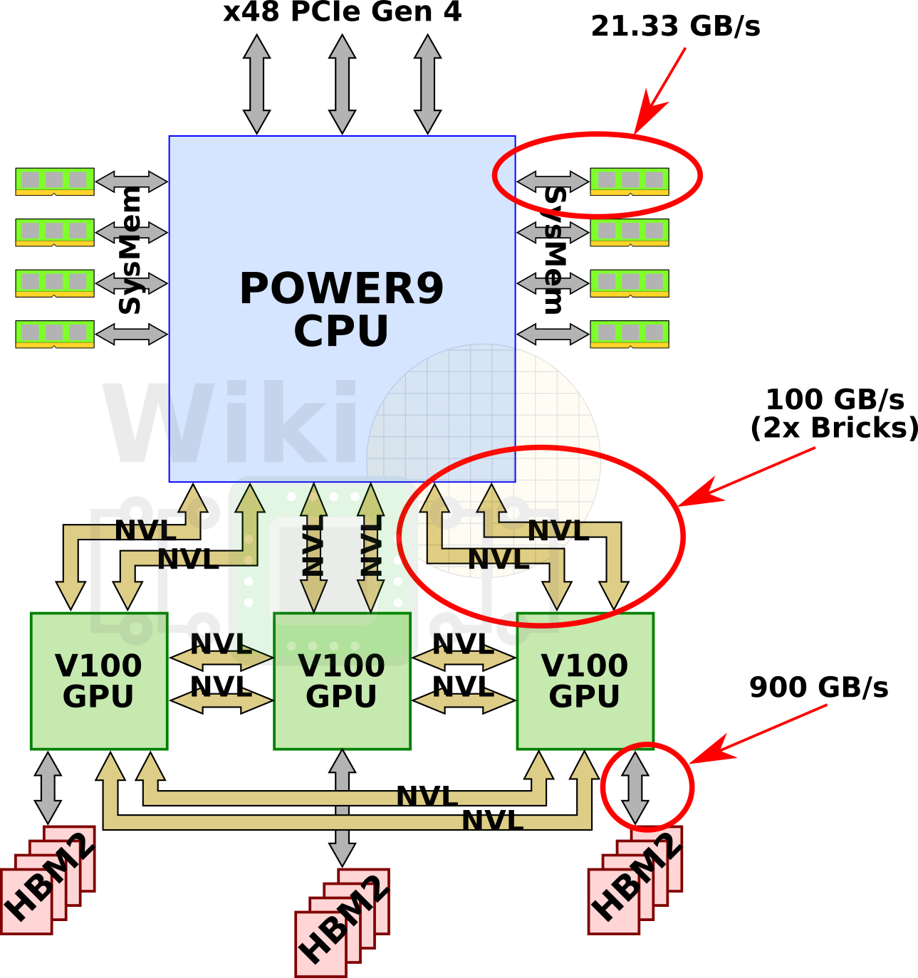
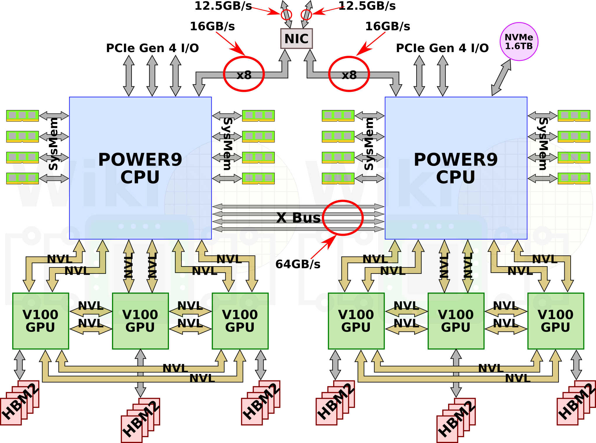
Each node has two 2200W power supplies, 4 PCIe Gen 4 slots, and a BMC card. There are two 22-core POWER9 processors per node, each with 8 DIMMs. For the Summit supercomputer, there are 8 32-GiB DDR4-2666 DIMMs for a total of 256 GiB and 170.7 GB/s of aggregated memory bandwidth per socket. There are three V100 GPUs per POWER9 socket. Those use the SXM2 form factor and come with 16 GiB of HBM2 memory for a total of 48 GiB of HBM2 and 2.7 TBps of aggregated bandwidth per socket.
Socket
We have recently discussed the NVLink 2.0 interconnects on the DGX-2. Since those systems use Intel‘s Xeon processors, the GPUs are connected to the CPU over PCIe switches. For Summit, the IBM POWER9 processors have native on-die NVLink connectivity meaning they are connected directly to the CPUs. The POWER9 processor has six NVLink 2.0 Bricks which are divided into three groups of two Bricks. Since NVLink 2.0 has bumped the signaling rate to 25 GT/s, two Bricks allow for 100 GB/s of bidirectional bandwidth between the CPU and GPU. In addition to everything else, there are x48 PCIe Gen 4 lanes for I/O.
The Volta GPUs have 6 NVLink 2.0 Bricks which are also divided into three groups. One group is used for the CPU while the other two groups interconnect every GPU to every other GPU. As with the GPU-CPU link, the aggregated bandwidth between two GPUs is also 100 GB/s.
Dual-Socket
There are two sockets per node. Communication between the two POWER9 processors is done over IBM’s X Bus. The X Bus is a 4-byte 16 GT/s link providing 64 GB/s of bidirectional bandwidth. A node has four PCIe Gen 4 slots consisting of two x16 (with CAPI support), a single x8 (also with CAPI support), and a single x4 slot. One of the x16 comes from one CPU, the other comes from the second. The x8 is configurable from either one of the CPUs and the last x4 slot comes from the second CPU only. The rest of the PCIe lanes used for various I/O applications (PEX, USB, BMC, and 1 Gbps Ethernet).
Full Node Capabilities
Each POWER9 processor operates at 3.07 GHz and supports simultaneous execution of two vector single-precision operations. In other words, each core can execute 16 single-precision floating-point operations per cycle. At 3.07 GHz, this works out to 49.12 gigaFLOPS of peak theoretical performance per core. A full node has a little under 1.1 teraFLOPS (DP) of peak performance from the CPUs and around 47 teraFLOPS (DP) from the GPUs. Note that there is a slight discrepancy between our numbers and ORNL’s. Buddy Bland, OLCF Program Director, informed us that their peak performance for Summit only include the GPU’s peak performance numbers because that’s what most of the FP-intensive code will use to achieve the highest performance. In theory, if we were to include everything, Summit actually has a higher peak performance of around ~220 petaFLOPS.
Every node has a 1.6 TB of NVMe Flash adapter and a Mellanox Infiniband EDR NIC attached.
| Full Node Capabilities | ||||
|---|---|---|---|---|
| Socket | Node | |||
| Processor | POWER9 | V100 | POWER9 | V100 |
| Count | 1 | 3 | 2 | 6 |
| FLOPS (SP) | 1.081 TFLOPS 22 × 49.12 GFLOPS |
47.1 TFLOPS 3 × 15.7 TFLOPs |
2.161 TFLOPS 2 × 22 × 49.12 GFLOPs |
94.2 TFLOPs 6 × 15.7 TFLOPs |
| FLOPS (DP) | 540.3 GFLOPS 22 × 24.56 GFLOPS |
23.4 TFLOPS 3 × 7.8 TFLOPs |
1.081 TFLOPS 2 × 22 × 24.56 GFLOPs |
46.8 TFLOPS 6 × 7.8 TFLOPs |
| AI FLOPS | – | 375 TFLOPS 3 × 125 TFLOPs |
– | 750 TFLOPS 6 × 125 TFLOPs |
| Memory | 256 GiB (DRR4) 8 × 32 GiB |
48 GiB (HBM2) 3 × 16 GiB |
512 GiB (DRR4) 16 × 32 GiB |
96 GiB (HBM2) 6 × 16 GiB |
| Bandwidth | 170.7 GB/s 8 × 21.33 GB/s |
900 GB/s/GPU | 341.33 GB/s 16 × 21.33 GB/s |
900 GB/s/GPU |
Compute Rack
There are 18 compute nodes per rack along with a Mellanox IB EDR Switch. Using a dual-rail Mellanox EDR IB interconnect, the nodes are connected in a three-level non-blocking fat-tree. Each node is equipped with dual-channel Mellanox InfiniBand ConnectX5 (IB EDR) NIC which supports 100 Gbps of bi-directional traffic. This card sits in a PCIe Gen4 shared x16 slot which is directly connected the two processors via x8 lanes. This enables each CPU to have direct access to the InfiniBand card, reducing bottlenecks.

With 18 nodes, each rack has 9 TiB of DDR4 memory and another 1.7 TiB of HBM2 memory for a total of 10.7 TiB of memory. A rack has a 59 kW max power and a total of 864 TF/s of peak compute power (ORNL reports 775 TF/s).
Full System
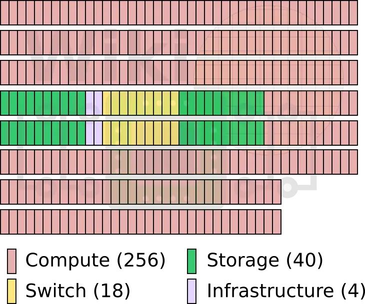
The full Summit supercomputer has 256 compute racks, 18 switch racks, 40 storage racks, and 4 infrastructure racks.
| Summit | ||||
|---|---|---|---|---|
| Rack | Compute | Storage | Switch | |
| Type | AC922 | SSC (4 ESS GL4) | Mellanox IB EDR | |
| Count | 256 Racks × 18 Nodes | 40 Racks × 8 Servers | 18 Racks | |
| Power | 59 kW | 38 kW | ||
| Summit, Peak Performance | ||
|---|---|---|
| Processor | CPU | GPU |
| Type | POWER9 | V100 |
| Count | 9,216 2 × 18 x 256 |
27,648 6 × 18 x 256 |
| Peak FLOPS | 9.96 PF | 215.7 PF |
| Peak AI FLOPS | 3.456 EF | |
| Summit, Memory | ||||
|---|---|---|---|---|
| Type | DDR4 | HBM2 | NVMe | |
| Node | 512 GiB | 96 GiB | 1.6 GB | |
| Summit | 2.53 PiB | 475 TiB | 7.37 PB | |
ORNL reports slightly more conservative numbers at around 200 PF and 3.3 EF peak performance for the GPU. Of course, peak performance is not the most interesting part. Real workload performance is far more important. Initial testing by ORNL has managed to achieve a peak throughput of 1.88 exaops of mixed precision while analyzing genomic data. This workload exploits the V100 tensor core matrix multiplication capabilities and is the highest performance reported to date.
The official TOP500 list will be announced in Frankfurt, Germany later this month (June 24-28). Assuming there are no surprises from China, Summit is expected to take the number one spot, dethroning the Sunway TaihuLight. Summit is also expected to do well on the Green500 list. However, due to its lower network injection bandwidth, Summit will have a hard time beating the K computer on the Graph500 list.
Summit Timelapse
ORNL has uploaded a Summit timelapse video.
Path to Exascale
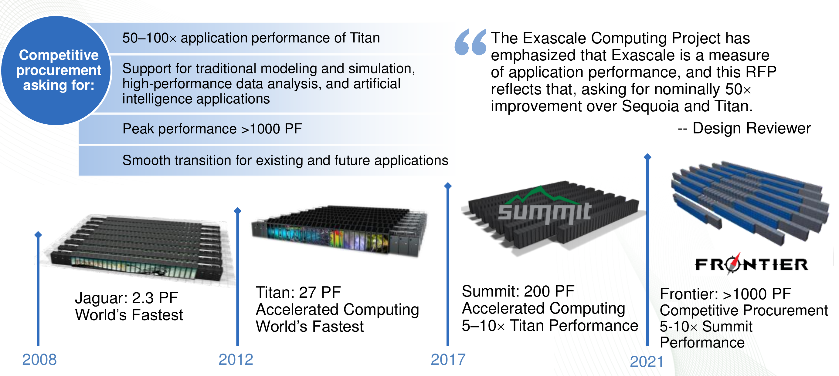
Summit is yet another stop on the way to Exascale. ORNL is expected to upgrade to a new Exascale supercomputer named Frontier. Frontier will have a theoretical peak performance of over 1,000 petaFLOPS or more appropriately defined as having 50-100x real application performance of Titan. In other words, Frontier should have around 5-10x the application performance of Summit.
–
Spotted an error? Help us fix it! Simply select the problematic text and press Ctrl+Enter to notify us.
–