
A Look At Celerity’s Second-Gen 496-Core RISC-V Mesh NoC
 For those who are not familiar with Celerity, this is a multi-university effort that has resulted in an open-source manycore RISC-V tiered accelerator chip. The project is part of the DARPA Circuit Realization At Faster Timescales (CRAFT) program which wants to drive the design cycle for custom integrated circuits to weeks and months from years. The Celerity team first presented the chip at Hot Chips 29. Last year, at VLSI 2019, Celerity was back to talk about the PLL and the NoC of its second-generation chip. The presentation was given by Austin Rovinski from the University of Michigan.
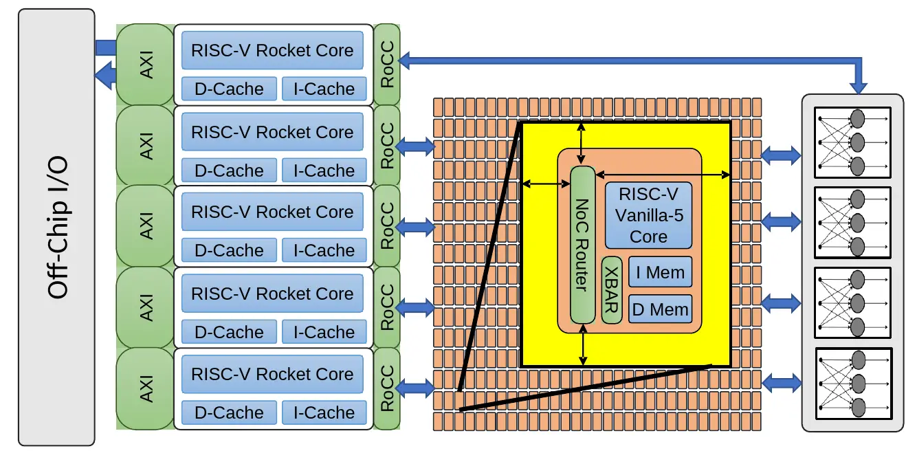
As a quick overview of the entire Celerity SoC, it’s a many-core multi-tier AI accelerator. At a high level, the chip comprises three main tiers – general-purpose, massively parallel, and specialization. Why a tiered SoC? To enable both high flexibility and higher power efficiency over a typical CPU design (albeit not quite as efficient as ASIC NPU). The general-purpose tier can pretty much do anything – general compute, memory management, and control the rest of the chip. For this reason, they have integrated five high-performance out-of-order RISC-V Rocket cores from the Free Chip Project. The next tier over is the massively-parallel tier which integrates 496 low-power custom-designed RISC-V cores in a mesh. Those custom cores, called Vanilla-5, are in-order scalar cores that take up 40x less space than a Rocket core. The last tier is the specialization tier that integrates a binarized neural network (BNN) accelerator. All three tiers are tightly linked and interfaces with DDR memory operating at 400 MHz.
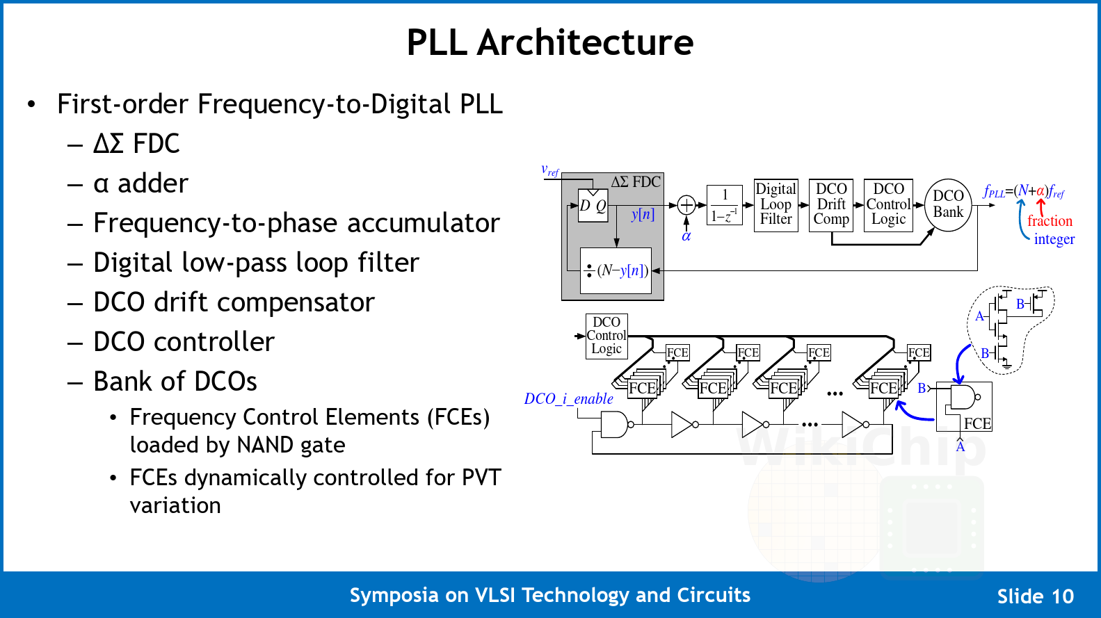
The manycore mesh clock on Celerity is supplied by a custom digital PLL. This is a fairly straightforward first-order ΔΣ frequency-to-digital converter (FDC) PLL. The implementation uses a bank of sixteen DCOs – each implemented as a ring oscillator with the inverting elements loaded with NAND gate FCEs as shown in the circuit diagram on the slide below. This was done in order to implement the entire design using only standard cells. To that end, the entire digital PPL is a fully synthesized and automatically placed and route design. The frequency range of this PLL on their 16-nanometer chip is 10 MHz to 3.3 GHz.
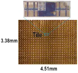
As with many academic projects, the silicon area is extremely important – the whole chip is 25 mm² (5×5). For Celerity, a number of key architectural design decisions were dominated by the need to restrict the silicon area which meant reducing the complexity. The manycore itself is an array of 16 by 31 of the tiny Vanilla-5 RISC-V cores. The what should have been the 32nd row of that array is used for the external host which is used to interface with the rest of the components on the chip (e.g., sending messages/data to the big Rocket cores for final processing). The entire mesh is 3.38 mm by 4.51 mm (15.24 mm²) or roughly 61% of the entire chip. The Vanilla-5 cores are a 5-stage in-order pipeline RV32IM cores so they support the integer and multiply extensions. In silicon, those cores are able to reach 1.4 GHz, 350 MHz higher than the first silicon they presented back at Hot Chips 29.
In order to reduce the complexity of the manycore array, Celerity makes use of partitioned global address space, single-flit packets, and a remote-store programming model.
The array utilizes a global partitioning address space (GPAS). In other words, instead of using caches, the entire memory address space is mapped across all the nodes in the network using a 32-bit address scheme. This approach, which also means no virtualization or translation, simplifies the design a great deal. They claim that compared to an equivalent coherent cache system, this design results in 20x lower area overhead. It’s worth pointing out that since the target workloads for this manycore array is AI acceleration (versus, say more general compute), they can get away with an explicitly partitioned scratchpad memory scheme as those workloads exhibit well-defined independent flow patterns that are highly parallel. Moreover, the ability to control the memory locality may prove to be quite advantageous for this type of code. Each core in the array can freely execute loads and stores to any local address, however, it can only perform stores to a remote address. No remote loads mean they cut the router area by 10% and since the remote stores can be pipelined, you prevent pipeline stalls. This remote store programming model scheme allows them to implement this using two networks – a data network and a credit counter network which is used for managing the outstanding stores.
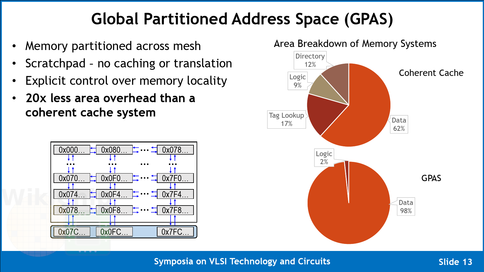
As we pointed out earlier, the 32nd row is used for the external host. In practice, this means that the memory mapping extends to the sixteen router stops at the bottom of the array which allows messages to get passed into and out of the manycore array to the big cores and other peripherals on the chip.
Instead of using wormhole routing which is very common for this type of application (also used by Kilocore, Piton, Tile64, at al.), Celerity incorporates the address and data into single flit packets. The design gets rid of the header/tail flits that would otherwise be needed to send both the data and metadata. Additionally, it gets rid of HOL blocking since there are no reserved routes. Each flit is 80b wide – 16 bit for control, 32 bits for the data, 10 bits for the node address and 22 bits for the memory address. The flit node address retains the ability to send data to any destination. The key benefit of this design is that since only a single flit is injected into the network, it enables the execution of one store per cycle with an in-order pipeline.
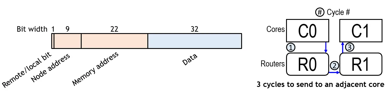
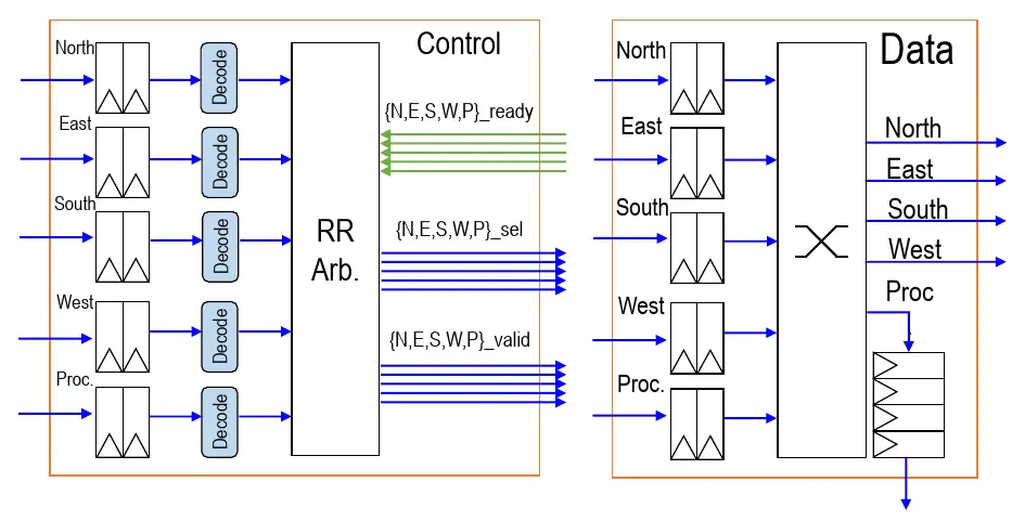
There is a router for each of the 496 notes in the manycore array. The router itself comprises two-element FIFOs at the input for each of the cardinal directions (N, S, E, W) as well as the control processor which are used as temporary storage in the event of network congestion. They use a round-robin arbitration for packet priority, allowing them to arbitrate every direction each cycle. They use dimension-order routing routes (reducing the offset in one direction before moving on to the other). The simple design allowed them to implement the entire router as a single-stage design with no pipeline registers inter-nodes. In other words, flits take just a single cycle per hop. For example, any adjacent core store has a latency of just 3 cycles – going to the local router, hopping to the neighbor router, and finally going to the neighbor’s memory space. The router sits on the same clock domain as the cores meaning they also operate at up to 1.4 GHz.
There are two networks – a data network and a credit counter network. The router employs a source-controlled credit counter which is decremented every time a remote store packet is injected into the network. Credits are returned over the credit counter network which uses the same architecture as the data described above but is just 9 bits since it just incorporates the node address.
So what does this all add up to? The Celerity team is reporting correct operations (on CoreMark) from 600 mV to 980 mV for frequencies ranging from 500 MHz all the way up to 1.4 GHz. We believe that Celerity is now the second-highest clocked University chip – just behind Kilocore (although it’s worth pointing out that due to packaging limitations, Kiloecore can only power 160 of its 1000 cores). At 1.4 GHz, the entire mesh has a maximum compute power of 694.4 INT32 GOPS. They report their numbers in Giga-RISC-V Instructions Per Second (GRVIS) instead of GOPS in order to highlight the fact that those are full RISC-V instructions instead of just integer operations. Note that since the Vanilla-5 cores are RV32IM, they support the RISC-V integer and multiply extensions but no floating-point support so all AI workloads must undergo quantization. Since the routers interconnecting the nodes sit on the same clock domain as the cores, with each router supporting routing 5 flits simultaneously each cycle, the total aggregated bandwidth per node is 748 Gbps for a total aggregated network bandwidth of 371 Tb/s.
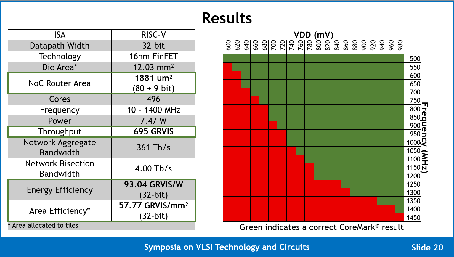
Unfortunately, the Celerity team did not report results for any common AI-related benchmarks. Instead, they opted to use CoreMark where they achieve 580.25 CoreMarks/MHz for a total score of 812,350. CoreMark has been the go-to comparison benchmark in the RISC-V community over the last few years. The problem with CoreMark is that it often produces incredibly optimistic scores for simple in-order designs that appear to compete well against well-tuned modern out-of-order designs while real-world workloads show massively different results. Given the premise of this chip is to produce a highly-flexible AI accelerator, we would like to encourage the Celerity team to produce more meaningful results such as an official MLPerf submission.
The open-source RTL for Celerity may be accessed on the Celerity website.
–
Spotted an error? Help us fix it! Simply select the problematic text and press Ctrl+Enter to notify us.
–