
A Look At Intel 4 Process Technology
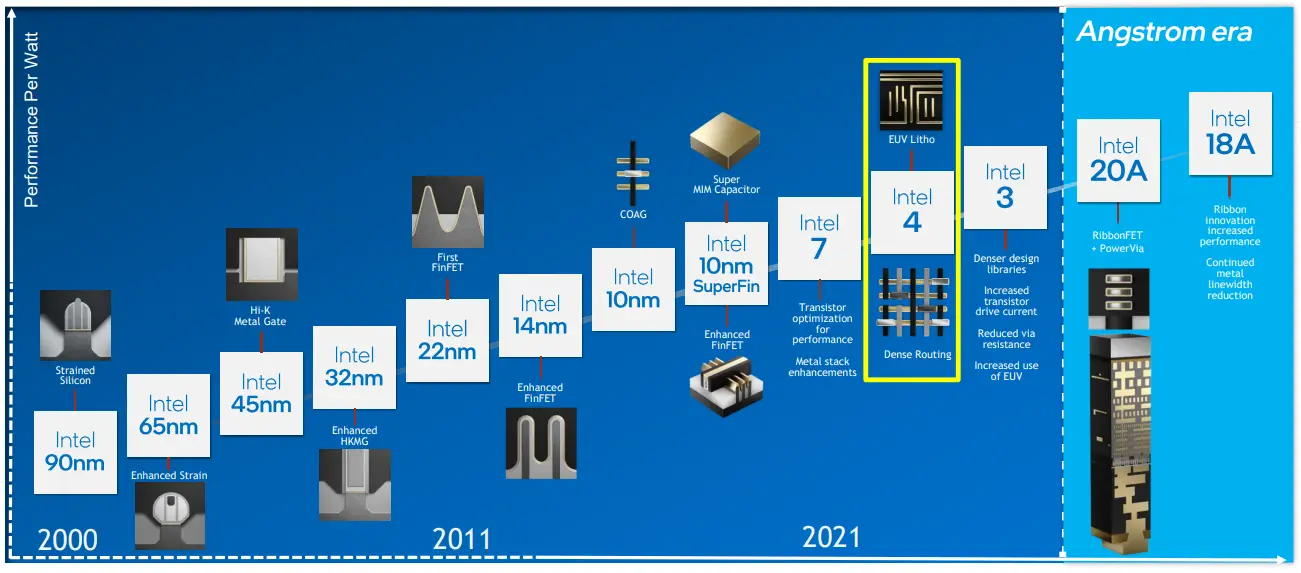
Back in early 2019, Intel finally publically acknowledged they screwed up – their ambitious 10-nanometer process was a bust; crazy density improvement goals along with too many novel technological features proved too much. The company pledged to correct this by going back to a more regular cadence of nodes through a more balanced PPA and measured risk-taking. It took two CEO switches, and under Gelsinger’s watch, we are finally seeing some of their initial effort to get back on track.

At the 2022 IEEE Symposium on VLSI Technology & Circuits which was held earlier this week in Hawaii, Intel presented a number of papers involving their Intel 4 process. The main paper was presented by Ben Sell, Vice President of Technology Development at Intel Corporation.
Intel 4
This new node is called Intel 4. For all practical purposes, it is the proper 10-nanometer successor. In other words, had it been released in 2020, it would have properly been called “7nm”. Today, it is called ‘Intel 4’ and is the successor to ‘Intel 7′ (formerly known as ’10nm Enhanced SuperFin’, formerly ’10nm++’).
Intel 4 is good but weird, really weird. Timing-wise, Intel expects this process to ramp up late this year – meaning products next year. If all goes as planned, ‘Intel 3’, the successor to Intel 4, will ramp almost exactly one year after (ramping in late 2023). This should start giving you an idea of how Intel sees this process. Before we delve into the details, we want to highlight that Intel 4 is not designed as a typical full-fledged node. While it’s a high-volume node, it is quite limited in what can be made on it (which will therefore likely limit its volume considerably). For example. It will not offer a number of large libraries you’d typically see from Intel nodes such as high-density and mid-range performance-density libraries that are important for things such as graphics and other applications but not CPU core designs. It’s for this reason that Intel 4 is producing the compute tile to be co-packaged with other chiplets made on different nodes.
Start Small, Get It Working, Build Up
Intel 4 represents a paradigm shift in the way the company approaches its node design. Historically, the company focused on rolling out what was traditionally called full nodes – a single node was introduced every roughly two years that brought a full generation worth of improvements. Foundries (e.g., TSMC as well as Fujitsu, Toshiba, NEC, and others a decade ago) used to introduce follow-up nodes called half-nodes that would bring further improvements to the node along with minor pitch scaling. The premise was simple: expending and enhancing an existing high-yielding node is both cheaper and easier.
See also: Process Technology History – Intel – WikiChip
While the traditional ‘full node’ and ‘half node’ model fell by the wayside. As recent FinFET nodes ballooned in complexity, foundries moved to a new ‘nodelet’ scheme. Under this model, a base node was to be introduced first (e.g., 7LPP or N7) which would then be succeeded by one or more enhanced nodes (nodelets) at an almost yearly cadence bringing small but incremental changes (e.g., N7P, N7+, N6, 6LPP).
Quickly succeeding Intel 4 is Intel 3 which is expected to ramp up late next year. The company said that process will introduce new libraries with further density, power, and performance improvement over Intel 4. Additionally, Intel 4 is forward-compatible with Intel 3, enabling easier design migration. More importantly, Intel 3 will boast a complete foundry offering. In many ways, Intel is taking a page from the foundry playbook. It’s clear that they are limiting the complexity of Intel 4 features and capabilities in order to mitigate risk. Furthermore, their ability to ramp Intel 4 this year will play a big role in their ability to bring Intel 3 to market on time next year. Proper execution is paramount. Building a broader, improved, portfolio of features, libraries, and other IPs on a more mature process is a lot easier and are the right way to go about this. This is critical given that Intel 3 is positioned as their initial flagship node for the Intel Foundry Services (IFS).
Given the limited scope of Intel 4 and its fast-follow full-fledged Intel 3 node, despite its full-node density/PPA characteristics, we think it’s best to think of Intel 4 as an interim stopgap node.
Products
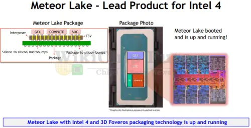
Originally, Intel revealed that both the Meteor Lake client SoC and the Granite Rapids data center SoC will be manufactured on Intel 4. However, earlier this year at the company’s 2022 Investor’s Meeting, the company announced that “it will upgrade Granite Rapids from Intel 4 to the Intel 3 process.” Given what we know today about the relationship between Intel 4 and Intel 3, the switch for Granite Rapids makes more sense today.
At technical conferences such as the IEEE VLSI Symposium, Intel typically limits the scope of their presentations to the technical aspects of their process exclusively. On this rather rare and unusual occasion, Sell talked about the first upcoming Intel 4 product – Meteor Lake. Meteor Lake with Intel 4 will be the lead volume product for 3D foveros packaging technology. Supporting the latest packaging technology, Intel 4 features the more aggressively-scaled micro-bump pitches for Foveros – scaling from 50μm to 36μm. Meteor Lake comprises a graphics tile, SoC tile, compute tile, and I/O tile all on a Si interpose. The Meteor Lake package and die shot is shown below.
Process Overview
Intel 4 (along with its enhanced version, Intel 3) is the last FinFET-based node from Intel. At a high level, this is the 4th major node to utilize FinFET after 22nm, 14nm, and 10nm. The process is said to utilize second-generation COAG and second-generation single dummy gate. Intel claims the new Intel 4 process offers around 2x area scaling for the high-performance library. Finally, it’s also worth highlighting that this is the company’s first EUV-powered process which is expected to enable significant process simplification.
- Extreme Ultraviolet (EUV) Lithography
- Self-Aligned Quad-Patterning (SAQP)
- Contact-over-active-gate (COAG)
- Single Dummy Gate (SDB)
- Enhanced Copper Interconnect
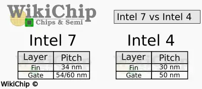
At the transistor level, the various pitches shrunk modestly. For example, compared to Intel 7, Intel 4 features a 30 nm fin pitch and a 50 nm gate pitch, a 0.83x and 0.88x shrink respectively. The interconnect stack underwent some more significant changes including a material change. The M0 metal pitch, for example, underwent a larger pitch shrink from 40 nm to 30 nm or 0.75x. We will revisit the interconnect a bit later.
Before we go further we wanted to reiterate that Intel 4 will only offer a high-performance cell library due to the limited products that will utilize this node. Typically, Intel designs at least three standard libraries for logic. For example, with Intel 10nm, the company had a high-density cell, a high-performance/mobile-performance cell, and ultra-high performance cells. While they utilized the same underlying transistors, they are characterized by the performance, power, and density characteristics which is a function of the pMOS and nMOS devices. For FinFET devices, this is a direct function of the number of fins. Therefore Intel 10nm had HD cells that can accommodate 2 fins per device, HP cells that could accommodate 3 fins per device, and UHP cells that can accommodate 4 fins per device.
Next Page (Scaling Is DTCO-Heavy)
–
Spotted an error? Help us fix it! Simply select the problematic text and press Ctrl+Enter to notify us.
–