
A Look At Intel 4 Process Technology
Interconnect
Intel 4 interconnect stack underwent considerable changes. A highlight of the basic design rules for Intel 4 is shown below. Compared to Intel 7 which had 17 metal layers, Intel 4 added one additional layer. Most of the interconnects above M4 saw the usual pitch shrink, most of which was around the 0.7x-0.85x scaling. As with the prior node, the two top layers are thick metal layers. By comparison to most other wires, Intel shrunk the very last thick metal layers quite substantially. The area that received the most attention is the first four routing layers. There, not only certain pitches did not shrink, some actually widened. Those layers also underwent new material changes.
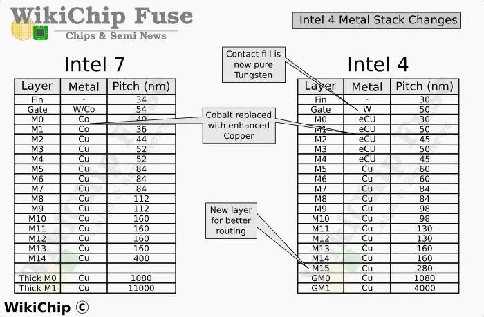
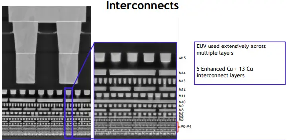
Although Intel did not detail the exact layers, both EUV and SAQP are employed at the tightest pitches. Additionally, a single damascene process is used to form the contacts for the M0 track, likely to facilitate EUV patterning at that step.
The four lowest metal layers span across the chip in two orthogonal directions and are used for cell-local power and routing. In Intel 4 they feature very regular pitches. There appears to be a good rationale for why some pitches shrunk while others widened and it’s mostly to do with cell layout optimization. In Intel 7, a very aggressive fin pitch for the M1 layer meant the company resorted to using a 3:2 pitch ratio. This had some quirk side-effects. In Intel 4, Intel actually scaled back the pitch by almost 1.4x to affix it to the gate through identical pitches. As we will show below, not only does this simplify design, it eliminated that layout quirk altogether. Intel appears to have done the same with the M3 layers. Our final observation here involves the M2 and M4 layers which also go parallel with the fins. Those feature a 2:3 ratio.
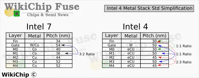
As we previously noted, in Intel 7, the company chose a very aggressive M1 pitch of 36 nm. This track runs parallel to the poly track. This pitch was chosen in order to facilitate a 3:2 ratio between the metal layer and the gate pitch. In other words, the tighter pitch allows for more M1 tracks per poly per cell which means a lot more pin hit locations. This design offered better inter-cell connections and better block-level access. Unfortunately, having this ratio at the M1 also resulted in a bit of a cell-level quirk where depending on the evenness/oddness of the cell poly count, you may end up with left or right-aligned cells. Honoring this problem meant a reduction in area utilization. Intel being Intel, the company “simply” duplicated the entire library to include an aligned and misaligned variant that could be substituted interchangeably where needed.

Intel 4 clearly dropped that scheme altogether for the sake of simplicity. Both the M1 and M3 layers are now pegged to the poly, eliminating this misalignment issue altogether. Interestingly, the company also pegged the M0 tracks to the fins. Those go perpendicular to the poly. The upper M2 and M4 layers which had a 44nm and 52nm pitch in Intel 7 both have a 45nm in Intel 4. The choice to go with 45nm is pretty clear from a layout perspective as they are now affixed to the fins at a ratio of 2:3. Keep in mind that since the cell height is a fixed property, there are no alignment issues going in that direction.
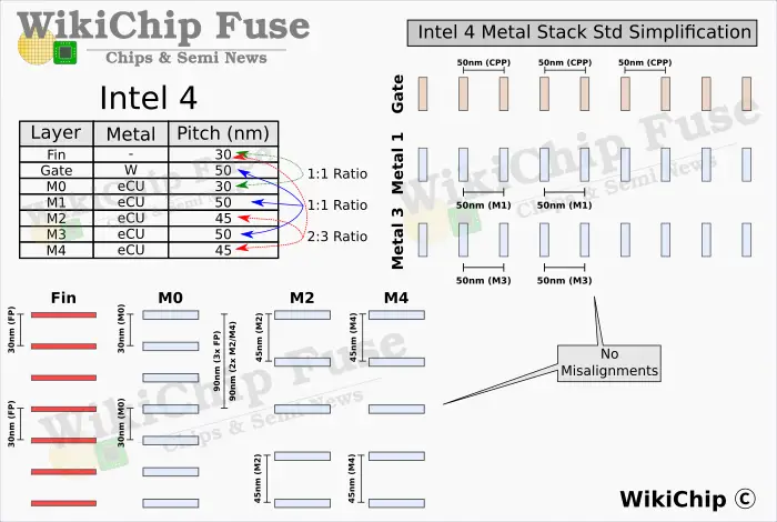
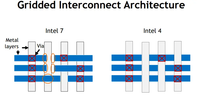
At VLSI Intel also discussed a new gridded interconnect architecture which is being introduced with Intel 4. In the prior node, Intel defined the minimum spacing for vias and track end caps. However, their exact placement was not specified. This resulted in a large number of patterns, introducing a new layer of analysis complexity due to the added pattern variability. In Intel 4, the line ends and vias are now strictly placed on a grid, reducing the possible placements. The new simple grid restrictions are said to improve yield through a reduction in pattern variability as well as through better identification of issues and optimization of the auto-place and route (APR) design flow.
Copper Is Back
When Intel first introduced their 10-nanometer process, they announced the introduction of new interconnects material – Cobalt. The primary motivation was for its better electromigration properties. As we continue to shrink the interconnect, the thickness of the high-resistivity liner and barrier for the copper interconnects stayed about the same. This is mostly due to the engineering difficulty in thinning it any further than the few nanometers it already is. The end result is that as the scale of the wire, the barrier itself starts making up a larger and larger share of the interconnect cross-sectional area. With the high-resistivity barriers slowly making up a larger portion of interconnect, it begins to dominate the resistivity of the wire itself. The result is an increased line and via resistance and ultimately electromigration reliability issues.
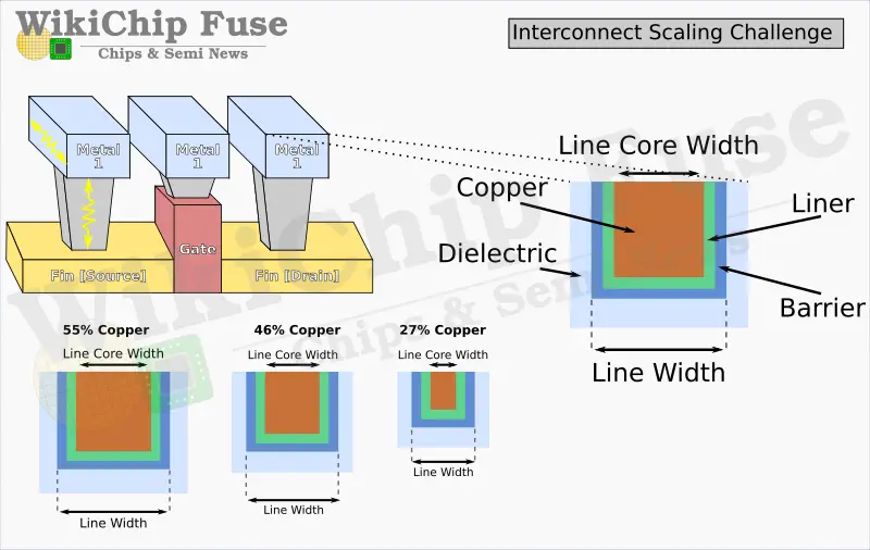
While the line resistance did increase in 10-nanometer, thanks to Cobalt and its thinner liner, at the two local interconnect layers (M0, and M1), Intel reported a 2x reduction in line resistance. Additionally, those two layers also so a 5-10x improvement in electromigration. Ultimately though, it seems that Intel is stepping back from Cobalt in Intel 4. Cobalt is a much more difficult material to work with and has been speculated to be one of the sources of their yield difficulties.
In the graph below, Intel demonstrated the relationship between Intel 7 with a pure Cobalt core with a Tantalum barrier versus a traditional Copper alloy core with a Tantalum nitride barrier. The two options had complementary attributes. The pure Co offered considerably better electromigration characteristics while offering worse line resistance. Likewise, the Cu alloy offered better line resistance but a worse electromigration lifetime. In fact, compared to pure Cobalt, the Copper alloy offered 0.75x the line resistance which is quite a large degradation in resistance. For Intel 4, the company chose to move to enhanced Copper (eCu) for the lowest four metal layers. This enhanced Cu wire comprises a Tantalum barrier with Cobalt cladding around a pure Copper core. All in all, eCu appears to be a middle ground win-win – offering much better EM lifetime versus Cu alloy (though not nearly as good as Cobalt) while offing a modest 0.85x improvement in line resistance.

–
Spotted an error? Help us fix it! Simply select the problematic text and press Ctrl+Enter to notify us.
–