
AMD’s Zen CPU Complex, Cache, and SMU
A lot has been written about the modularity of AMD’s latest Zen microarchitecture; specifically how a single die, a Zeppelin, can scale from the mainstream consumer market all the way to the high core-count server market. One of the key ingredients that helped facilitate the design of the Zeppelin is the CPU Complex (CCX).
This article assumes the reader is familiar with AMD’s recent “Zen” core. As a refresher, we recommend skimming through our Zen microarchitecture article.
CPU Complex (CCX)
A CCX is a complete macro block consisting of a number of independent Zen cores, their private level 2 cache, and a shared level 3 cache. A single die may instantiate multiple CCX blocks to build a larger core count design. The full CCX configuration has four Zen cores, their accompanying L2 banks of 512 KiB each, and 8 MiB of shared level 3 cache. That configuration consists of 1.4 billion transistors and occupies 44 mm² using GlobalFoundries 14LPP FinFET process.
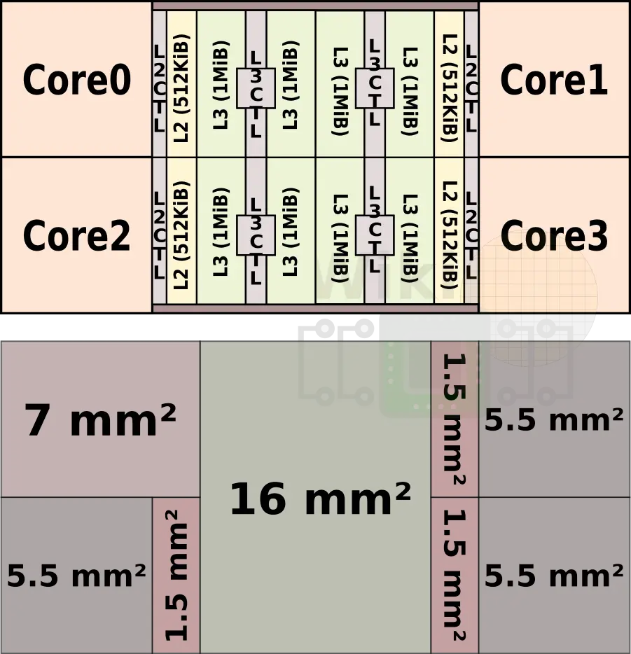
The level 3 cache makes up 36.5% of the CCX at 16 mm² while each core makes up the remaining 7 mm² which includes the 1.5 mm² private L2.
Variants
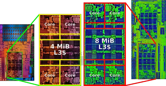
The complex itself is fairly configurable. For the mainstream Zeppelin, the full configuration is used. For client products that do not require the large L3 cache, a variant with half the L3 (4 MiB) can be used. Interestingly, AMD noted that a third variant for the cost-sensitive and low-power market is also available which incorporates just two cores with a smaller L3 cache. AMD has yet to announce any products that make use of the dual-core option, but at least we now know the configuration officially exists.
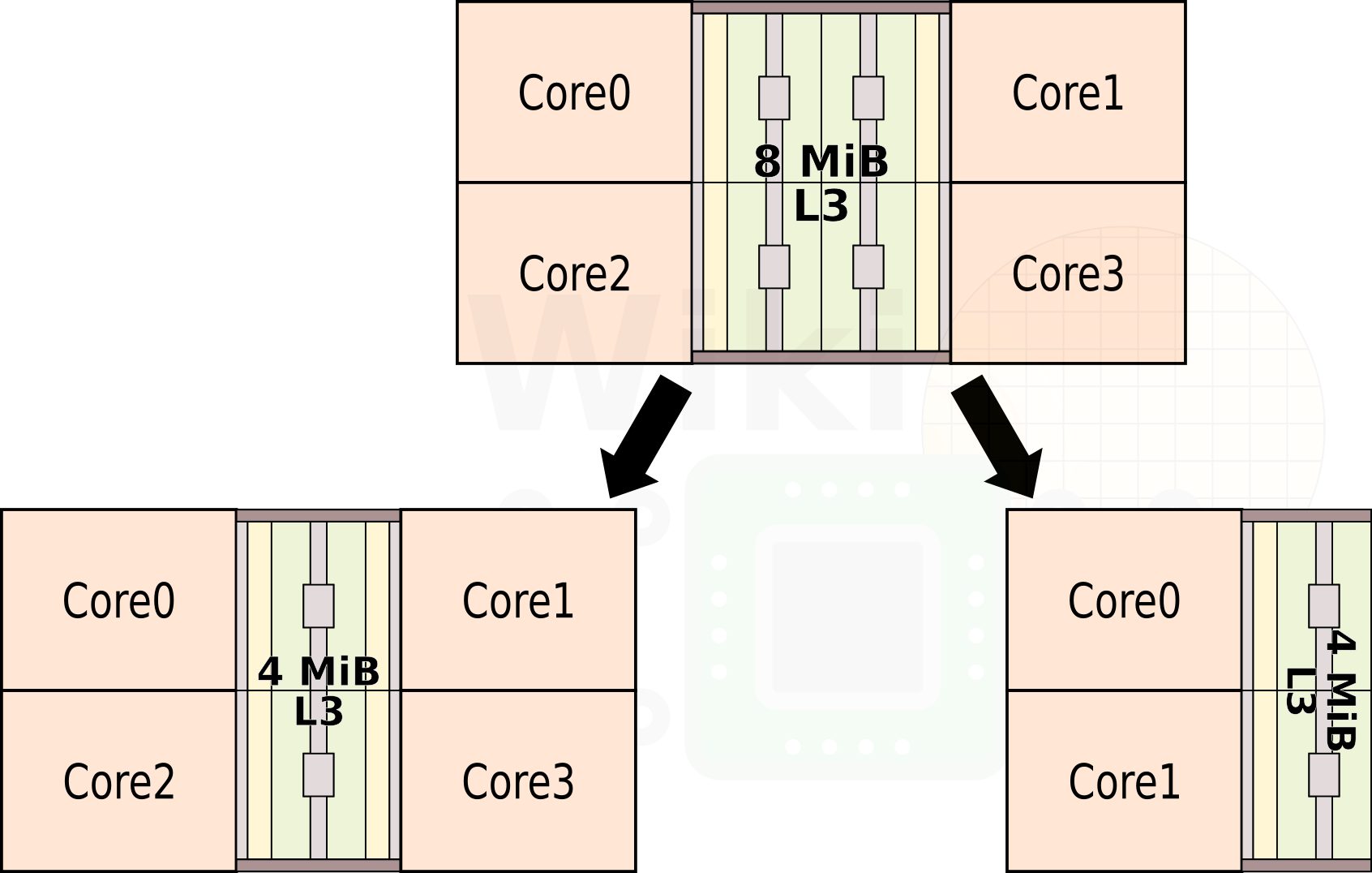
The full CCX (8 MiB L3$) variant can be found in mainstream desktop processors (Summit Ridge) whereas the reduced cache variant is found in the mainstream processors with Radeon Vega GPUs (Raven Ridge).
Design
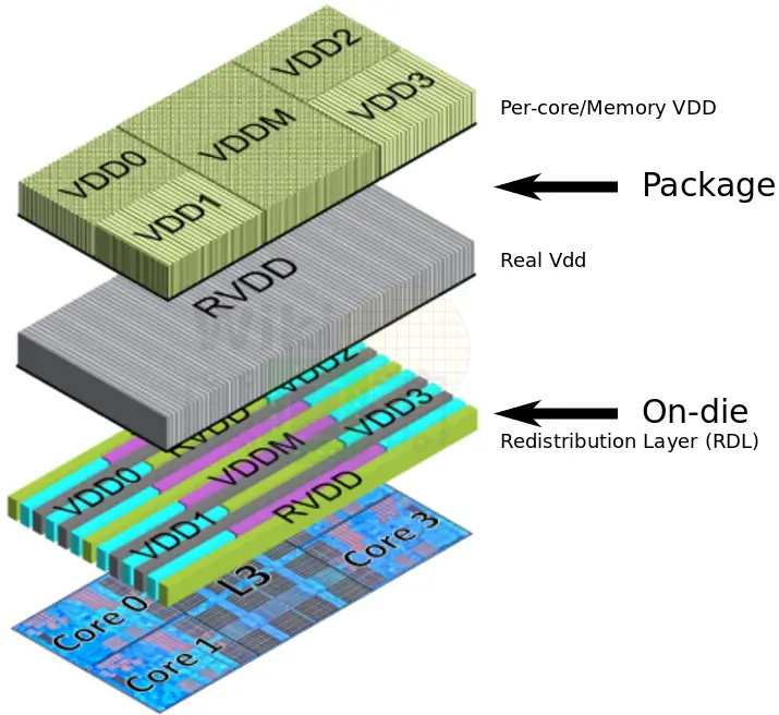
To improve the design and allow for finer voltage control, the core complex is made of multiple voltage domains. The real VDD (RVDD) is fed from the VRM into the chip which is distributed in the package to the individual cores as well as the SRAM peripheral logic. Each of the Zen cores has its own local low drop-out regulator that takes the RVDD as input, forming its own voltage domains. At the package-level, the RVDD is controlled by a platform voltage regulator with a granularity of 6.125 mV whereas the LDOs supply the individual cores with a much finer granularity of 2 to 3 mV per step. In addition to the cores, the L2 and L3 SRAM bit cells are independently powered by a separate VDD,M in order to allow greater voltage ranges for the cores. Because the RVDD package plane over the shared L3 cache is also shared with the individual cores, an additional on-die redistribution layer (RDL) is used for routing the VDD,M to the L2 SRAM macros across the L3-core boundary.
Prior to Zen, AMD had two entirely separate microarchitectures for the ultra-low power and high performance. With Zen, AMD has combined the two design targets, optimizing for multiple markets. The main optimization point was at the 1 V where the performance per watt was optimized. This is also the area where server SKUs are also located. The mainstream/performance desktop models, where SKUs are pushing into the FMAX region, the design was focused on RC-dominated paths. Since VMAX is considerably higher than the nominal voltage, significant analysis of gate and intra-dielectric breakdown was necessary. On the other side of the scale, in mobile and fanless models, the design was focused on gate dominated paths and roll-off at low voltages.

–
Spotted an error? Help us fix it! Simply select the problematic text and press Ctrl+Enter to notify us.
–