Intel Unveils Foveros Omni And Foveros Direct; Leveraging Hybrid Bonding
Intel unveils the Foveros Omni and Foveros Direct packaging technologies; which will be leveraging multiple base dies and hybrid bonding
Read more
Your Chips and Semi News
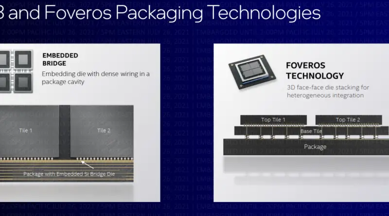
Intel unveils the Foveros Omni and Foveros Direct packaging technologies; which will be leveraging multiple base dies and hybrid bonding
Read more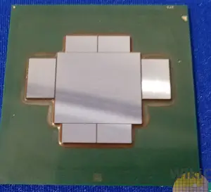
A look at ODI, a new family of packaging interconnect technologies that bridges the gap between Intel’s EMIB (2.5D) and Foveros (3D) by providing the flexibility of an EMIB in 3D with additional benefits of thermal & power.
Read more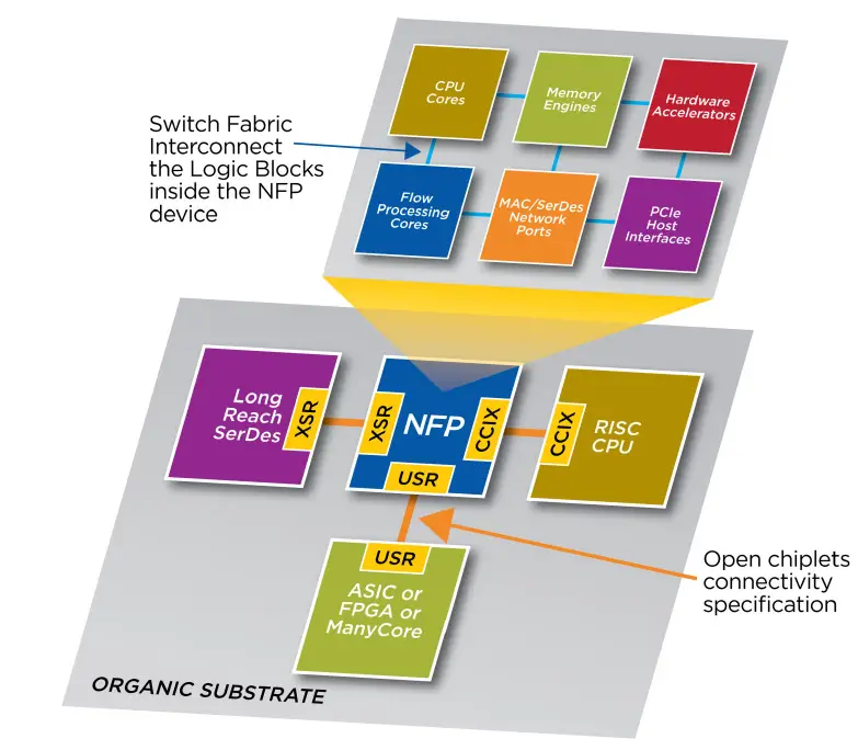
Jumping ahead of emerging semiconductor trends, the OCP new Open Domain-Specific Architecture subgroup makes a push for an open and standardized chiplet interface and marketplace.
Read more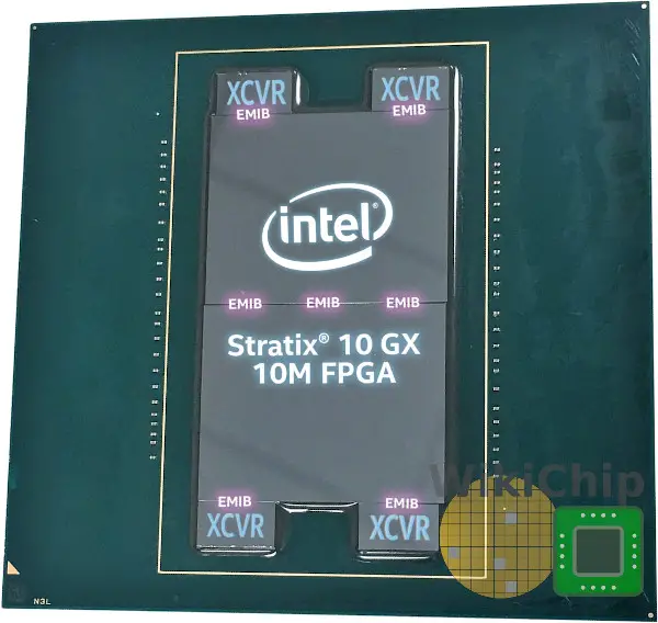
Intel launches the industry’s highest-capacity FPGA; 10-million LEs comprising two large FPGA dies interconnected using the company’s 2.5D EMIB packaging technology.
Read more
Intel launches a new Stratix 10 family bringing new support for PCIe Gen 4.0, new cache-coherency support, and Optane DC DIMM support.
Read more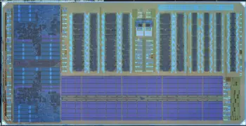
From a DARPA vision and a $15 million seed to a commercialized CMOS silicon photonics product: how Ayar Labs collaboration with GF produces a photonics chiplet that can supercharge Intel FPGAs.
Read more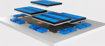
Intel is expanding its packaging portfolio with more advanced 2.5D and 3D technologies including multiple 3D stacks and omnidirectional interconnects.
Read more
An outline of Intel’s process technology and packaging plans including their 10nm and 7nm nodes as discussed at the company’s recent investor meeting.
Read more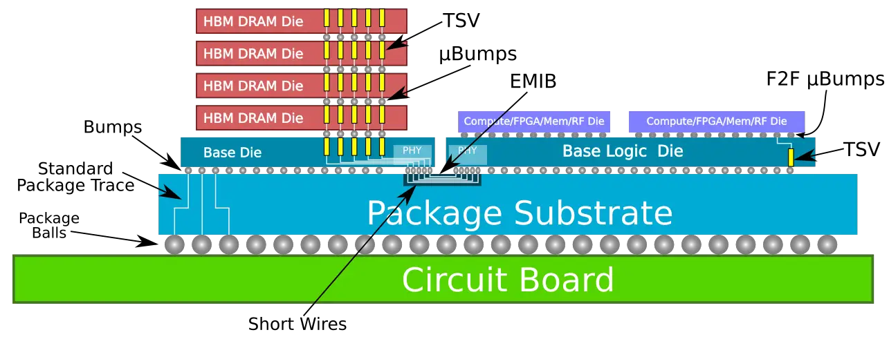
At the recent Intel Architecture Day, the company unveiled their latest advanced packaging technology called Foveros, a face-to-face three-dimensional (3D) die stacking packaging technology in an effort to assist with the slowing of Moore’s Law.
Read more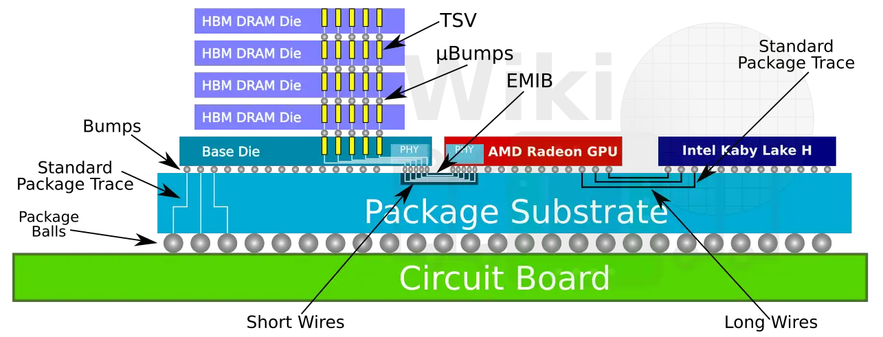
A look at Intel’s current generation of Thin & Light processors with high-performance graphics, formerly known as Kaby Lake G, from Hot Chips 30.
Read more