
Intel Launches Stratix 10 GX 10M; 10M LEs, Two Massive Interconnected Dies
Earlier this week Intel unveiled the latest device in its Stratix 10 family – the Stratix 10 GX 10M. The new device features 10.2 million LEs making it the industry’s largest FPGA in production. Intel says that the device has been sampling for quite some time and has now entered production.
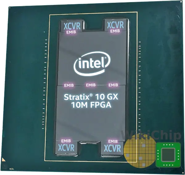
Stratix 10 GX 10M
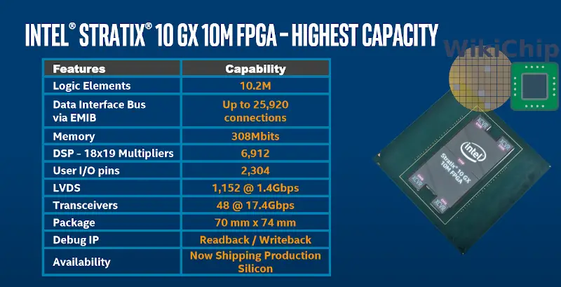
The Stratix 10 GX 10M is a very interesting device for a couple of different reasons. First, it’s huge -it’s Intel’s largest of the large FPGAs, packing 10.2 million logic elements. This FPGA is primarily aimed at large-scale ASIC prototyping and emulation and for those applications, no amount of logic is enough. This device goes head-to-head with Xilinx’s Virtex UltraScale+ VU19P which was announced back in August. Intel’s new FPGA is roughly four times the capacity of its prior largest-capacity FPGA. Given the compact nature of the device, Intel is reporting up to 40% lower power consumption compared to using four Stratix 10 GX 2800 FPGAs with comparable capacity at an fmax of 50 MHz with a 12.5% toggle rate.
In addition to the large raw compute, this device features 6,912 18×19 multipliers which equate to 3,456 variable-precisions DSPs blocks. There are also up to 48 full-duplex transceivers with data rates up to 17.4 Gbps data rates chip-to-chip and presumably 12.6 Gbps backplane. Both of those features are comparable to existing Stratix 10 devices.
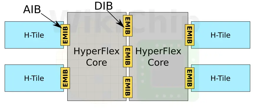
EMIB For Logic-to-Logic
Up until now, Intel has been using its EMIB packaging technology to connect a single logic die to memory and I/O. For example, the Stratix 10 DX which was announced in September can have up to 2 HBM2 stacks and four transceivers tiles. Previously Intel also connected the HBM2 stack to the AMD Vega M GPU using an EMIB.
With the new Stratix 10 GX 10M Intel has taken the next major step – connecting two large, high-power, logic dies together an EMIB. The dies themselves are also new, designed with tighter bumps on the perimeter between the two dies for the EMIB interface. In terms of capacity, the dies are considerably bigger than the prior Stratix 10 – each with 5.1 million LEs, with a total of 43.3B transistors for both. That’s almost twice as many LEs per die as existing devices. It also happens to come close to the number of LEs Intel had originally promised when it announced the Stratix 10 family back in 2015.
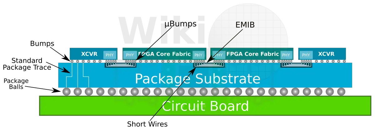
Looking a bit deeper into the packaging interconnect. The package itself is very large, measuring 70 mm x 74 mm. The two FPGA fabric dies are interconnected using three embedded bridges. There are a total of 25,920 parallel connections between the two dies. One thing to point out is that unlike the connections to that XCVR and HBM tiles which use the AIB and UIB interconnects respectively, the connections between the two FPGA fabrics use the brand new DIB interconnect. More information about this interconnect will be disclosed in the future.
Related Stories
- Intel Stratix 10 DX Adds PCIe Gen 4.0, Cache Coherency: UPI As Stopgap
- Hot Chips 30: Intel Kaby Lake G
- DARPA ERI: How Ayar Labs Collaboration With GF Produces A Photonics Chiplet That Can Supercharge Intel FPGAs
- Left, Right, Above, and Under: Intel 3D Packaging Tech Gains Omnidirectionality
- Ayar Labs Realizes Co-Packaged Silicon Photonics
–
Spotted an error? Help us fix it! Simply select the problematic text and press Ctrl+Enter to notify us.
–