
A Look at Spring Crest: Intel Next-Generation DC Training Neural Processor
This year at Hot Chips 31, in addition to the Nervana NNP-I inference accelerator, Intel also presented its next-generation data center training accelerator – the Nervana NNP-T. The chip was presented by Andrew Yang, Intel Senior Principal Engineer and the lead of the training product architecture in the AI products group. Yang is one of the original Nervana team members where he was the Senior Director of Hardware.
Please note that some of the information in the article comes from other sources such as the Kloss’s Nervana presentation from the Linley Processor Conference form early this year. Carey Kloss is VP of Intel AI Products Group and GM for AI Hardware.
Spring Crest
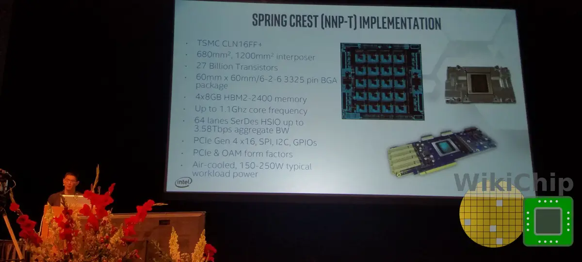
Spring Crest is the successor to Lake Crest which was the original 28-nanometer Nervana NPU. While the original chip served as a learning experience and prototype that only sampled to select customers, Spring Crest targets mass production. The chip is branded as the Nervana Neural Network Processor for Training (NNP-T) 1000.
 Spring Crest is a training neural processor for the data center. It is intended for air-cooled infrastructure in the 150-250W typical power range. The final product will come in two form factors: a PCIe accelerator card and an OCP mezzanine accelerator module. Communication between the chip and the host CPU is done over 16 lanes of PCIe Gen 4, enabling close to 32 GB/s of bandwidth.
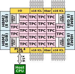
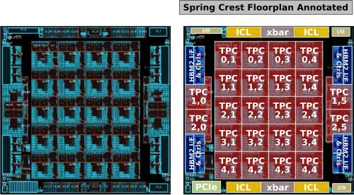
At a high level, Spring Crest comprises 24 tensor processor clusters or TPCs. Note that those were previously called Compute Clusters (CCs). There is 60 MiB of tightly-coupled scratchpad memory distributed among the TPCs. Spring Crest features 32 GiB of near-chip memory in the form of HBM2 operating at 1200 MHz. In order to support scale-out, there are four InterChip Links (ICLs) comprising 64 SerDes lanes. Communication is done over a 2D mesh NoC that interconnects all the TPCs together as well as to the HBM2 stacks and the various I/O peripherals.
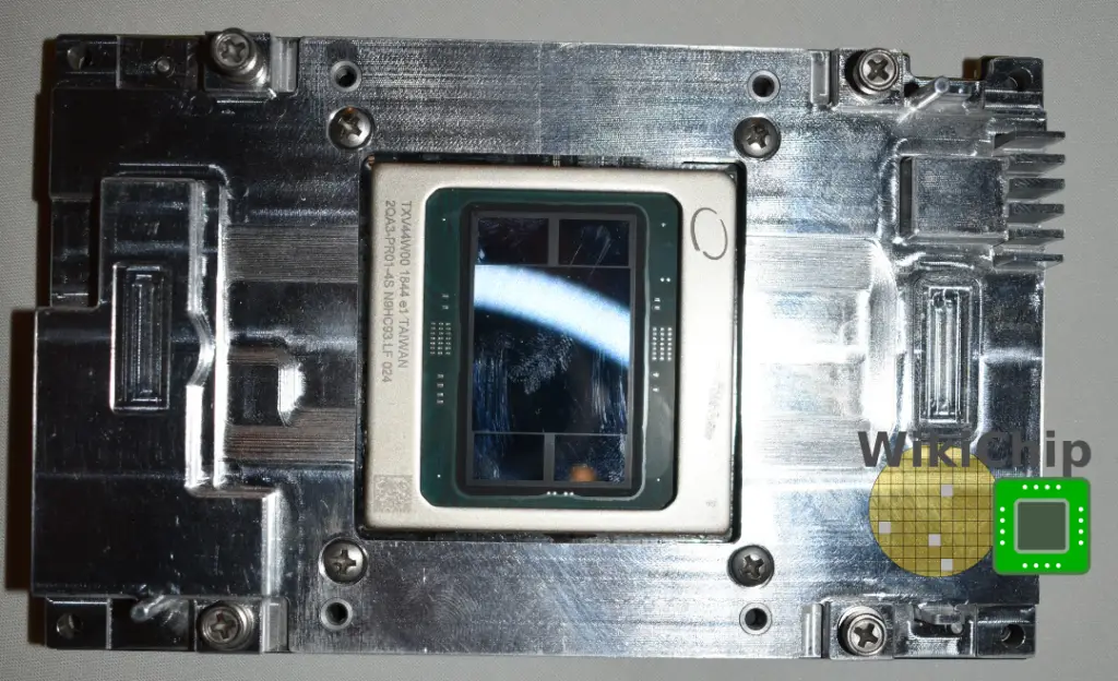
The chip itself is fabricated on TSMC 16-nanometer process (16FF+), packing 27 billion transistors on a 680 mm² die. Spring Crest uses a 2.5D CoWoS package which includes four 8-Hi HBM2 stacks on a 1200 mm² interposer. The package itself is standard 6-2-6 layer stackup 60 mm x 60 mm BGA package with 3,325 contacts.
Intel says that the chip will come with models up to 1.1 GHz and up to 119 TOPs (bfloat16).
Processing Units
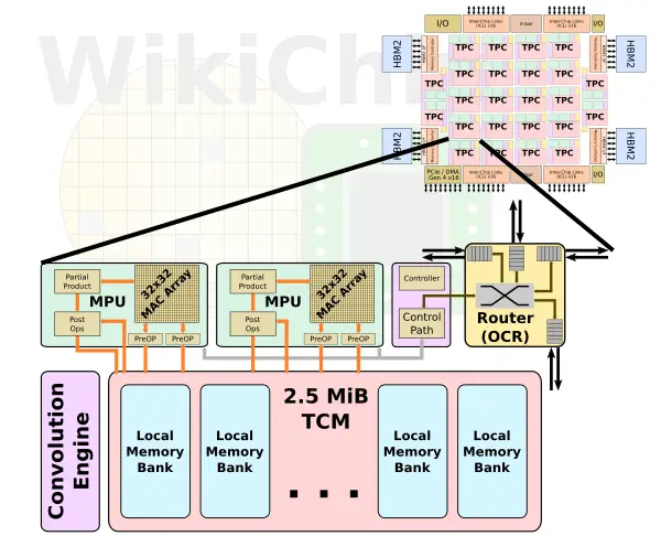
The workhorse processing units on Spring Crest are the Tensor Processing Clusters (TPCs). There are 24 instances of the TPC on a chip. If we look closely at the floorplan that Intel published we can see that 20 of the TPCs use one physical layout in a 4×5 grid while four additional TPCs use a second physical layout slightly rearranged to fit between the two HBM interfaces on the east and on the west side of the die.
Each Tensor Processing Cluster comprises two MAC processing units, a control unit, a convolution transformation engine, a highly-banked tightly-coupled memory, and a crossbar on-chip router (OPC).
The TPC is a cluster of two identical processing units. Each unit has two major components: a matrix-multiply core and a vector pipeline. The matrix multiply core is a 32×32 array that uses bfloat16 for the multiply and FP32 for the accumulate. We have seen Intel choosing a 32×32 array with its Spring Hill inference chip as well (though keep in mind, Spring Hill uses Int8 while Spring Crest uses BF16). The choice for 32×32 is the good balance they get between high data reuse and problems with quantization effects. In total, the chip has a theoretical peak compute of 4096 OPS/cycle per TPC, and with 24 TPCs, we are looking at 98.3 KOPS/cycle (or 98.3 TOPS at 1 GHz).
Outside of the matrix-multiply core is the vector pipeline. It is designed to reduce memory pressure and improve power efficiency. The pipeline performs multiple operations on a set of inputs and intermediate values. The vector pipeline supports both FP32 and BF16 and offers specialized optimizations for things such as activation functions, random number generation, reductions, and accumulations.
From Flexpoint to Bfloat16
One of the big changes from the original Nervana Lake Crest chip is the switch from Flexpoint to bfloat16. Flexpoint was essentially a block integer format with the exponent split off and shared across all the applicable execution units. The idea was that since the exponent is identical across all the relevant compute elements, operations such as addition and multiplication can be done as a fixed point operation.
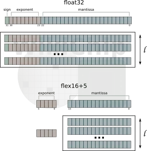
Yang was asked about Nervana’s decision to switch to bfloat16. “We initially designed Flexpoint on our first chip. What we found was that it was difficult for our software, not our chip, to scale out. When there was more research into numerics and we discovered bfloat, we decided to pivot to bfloat that time,” Yang answered.
By reducing the mantissa but preserving the exponent field the same size as FP32, you maintain the same dynamic range. Bfloat16 provides a good balance in area and power efficiency while being easy to converge without sacrificing accuracy.
Memory Subsystem
The memory subsystem within each TPC is rather large, having 2.5 MiB of SRAM. The scratchpad memory is highly-banked and multi-ported, designed for simultaneous read and write accesses. This memory does sourcing and sinking of data with the compute blocks as well as the routing mesh. There is a total of 1.4 Tbps of bandwidth between the compute blocks and the scratchpad memory banks. A lot of the magic here is actually in the software. Yang said that the hardware management of memory has been kept to a minimum in order to not interfere with software optimizations. To that end, the software explicitly manages the memory to optimize data locality and data residency. Message passing, memory allocation, and memory management are all under software control. It’s worth noting that this applies to both the on-die scratchpad memory and the off-die HBM memory; the software can directly transfer memory between the TPCs as well as from and to the HBM.
–
Spotted an error? Help us fix it! Simply select the problematic text and press Ctrl+Enter to notify us.
–