N3E Replaces N3; Comes In Many Flavors
Earlier this summer TSMC held its 2022 Technology Symposium where the company shared some details about its upcoming 3-nanometer node.
N3
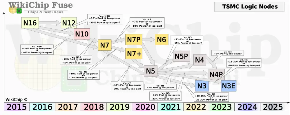
The first 3-nanometer node from TSMC is the “N3” node. This node was announced back in 2018-2019 and is planned for the second half of this year. Numerous articles seemed to have been published online claiming this node was delayed but as we first wrote about N3 in early 2019, TSMC has always planned for N3 to ramp in the second half of 2022. The confusion appears to rise from an earnings call discussion last year that explained that the N3 ramp date is slightly longer than prior nodes in order to align with specific customers’ products. Nonetheless, we do not see any delay with their current ramp plans and the current schedule is largely consistent with what the company outlined 3 years ago.
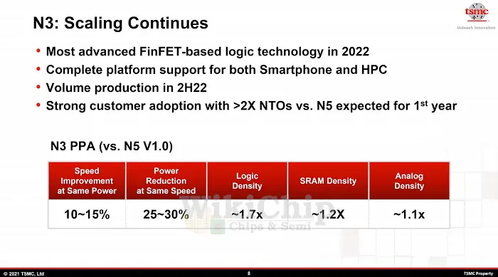
The N3 node is planned for the second half of this year with announcements expected this month or around October. The N3 node remains a FinFET device, as with prior nodes. The company says it sees good yields. When compared to TSMC’s Vanilla N5 node, the original N3 node is said to deliver around 10-15% improvement in speed at ISO-power or, alternatively, 25-30% reduction in power at ISO-speed (both at nominal 0.75V). At the core level, TSMC claims around 1.7x density improvement in digital logic and around 1.1x improvement in analog logic. N3 also offers a rather lackluster SRAM bitcell scaling of just ~1.2x improvement.
Two Steps Forward, One Step Back?
The N3 node is weird. It is TSMC’s first 3-nanometer class process technology, but it won’t be the mainstream node everyone will utilize. In fact, it appears to be a one-off node that the company abanded sometimes prior to rollout. It looks as if TSMC engineers encounter some roadblocks along the way and decided to change things mid-way. We say all of this because TSMC moved on to a whole different node this year called “N3E” which we discuss below. Most of the messaging at the Technology Symposium was about N3E with the original N3 node getting just a brief pass-by mention. The big takeaway here is that N3E is a very different node from N3. While the nitty-gritty node details have not been disclosed, at a high-level it has different PPAs along with what the company claims are “very different” design rules intended to improve yield. The result of this is that N3E will not offer any direct migration path from N3, making N3 sort of a dead-end node for designers which is why TSMC expects most customers to utilize N3E instead. So why N3 exist at all? The easiest explanation is to satisfy customers’ commitment to those early technology adopters. Long term, the initial N3 node will likely fade into obscurity.
N3E
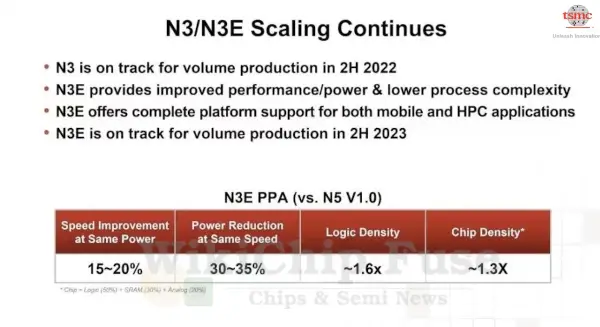
All of this leads to the N3E node, an “Enhanced N3 node”. Mentioned publically for the first time last year, N3E is included under TSMC’s umbrella marketing “N3 Family”; albeit N3E is very different from N3. The design rules are said to be very different and the IP is implemented differently enough to make them incompatible design-wise. For customers, there is also no direct IP migration path for designs made on N3 to move to N3E. Put simply, N3E is everything N3 apparently was supposed to be. TSMC says the new node included “significant changes” over N3 that produced different PPAs along with better yield through “lower process complexity”. For this reason, TSMC’s broader IP ecosystem targets N3E. TSMC says that, unlike N3, N3E “will offer complete platform support for both smartphone and HPC applications.”
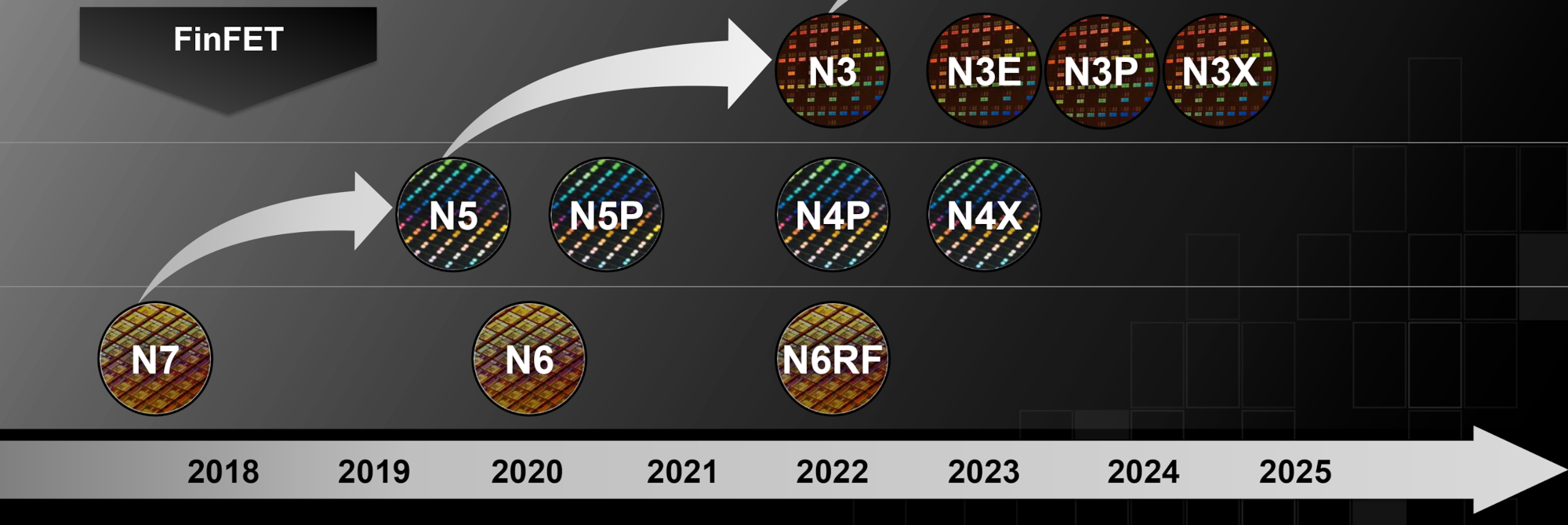
Offering a complete foundry IP ecosystem, N3E will serve as the main foundry node for TSMC 3-nanometer class chips. Like the original N3, the N3E node is also a FinFET device. TSMC says the node is already design-ready with PDK 0.9 already at the customer’s hand. N3E is scheduled for around one year after N3, putting it firmly around the second half of 2023. As we noted earlier, N3E differs significantly enough from N3 to be treated as an entirely different migration path from N5. TSMC also makes its comparisons for N3E against N5 and not N3 for this very reason.
To that end, compared to N5, N3E is said to offer around a 1.6x density improvement in digital logic and around 1.1x improvement in analog logic. The slight density regression is noteworthy. TSMC says that N3E will enjoy higher yield from the get-go and offer better performance and power characteristics – 15-20% improvement in speed at ISO-power or, alternatively, 30-35% reduction in power at ISO-speed (both at nominal 0.75V). Both values are around 15% higher than N3.
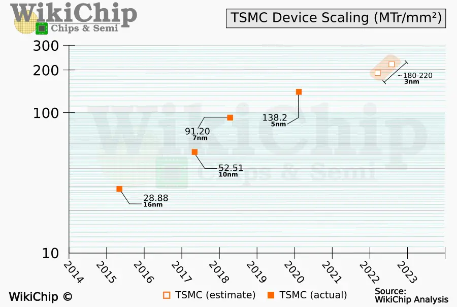
In terms of density, given that TSMC has not publically disclosed any of the design rules, we put a rough range estimate of around 180-220 MTr/mm2 with N3E slightly below the N3 density. It’s worth highlighting that density estimates gets somewhat more complex even when utilizing our usual .6 NAND2 + .4 SSF metric because of FinFlex (detailed below) which allows for higher variance in densities across blocks and chips. It should be noted that TSMC itself added a new metric to their N3E slide above called “Chip Density” which the company derives using “50% [Logic Density] + 30% [SRAM Desnity] + 20% [Analog Density].” TSMC says the “chip density” is ~1.3x versus the 1.6x logic density for N3E vs N5.
FinFlex – Mix’n’Match Cell Library
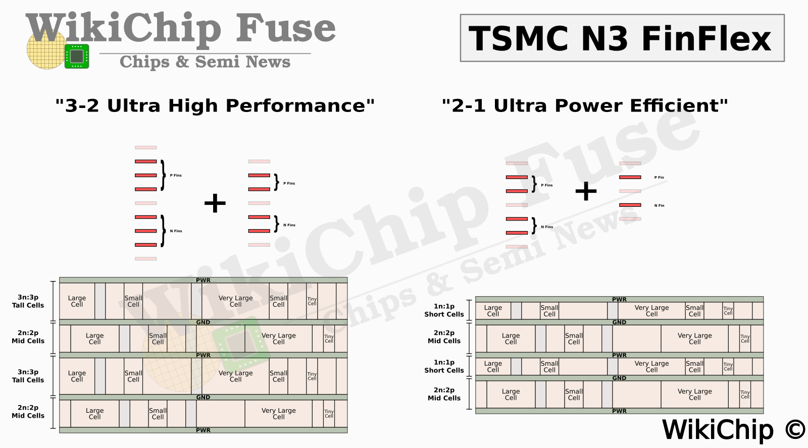
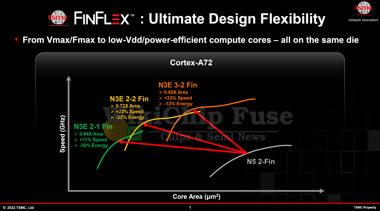
One of the more interesting announcements that came out of the symposium is the announcement of “TSMC FinFlex”. Within the N3E node, TSMC offers a number of standard cell libraries that offer a varying compromise of power, performance, and area. Those libraries include HP, Mid, and HD cells that comprise 3:3, 2:2, and 1:1 fin ratios. Under FinFlex, TSMC offers the ability to abut across power rails certain combinations of cell heights together, under a set of design rules, in order to achieve additional design characteristics not possible when using any single library exclusively. In other words, this technique is designed to offer a more granular mixing of multiple cell libraries in order to achieve better performance or power characteristics. Specifically, TSMC announced two options: “3-2 Ultra High Performance” for highest performance applications and “2-1 Ultra Power Efficient” for ultra power efficiency.
Below are some tradeoffs of the various options on the same industry standard Cortex-A72 implication across N5 vs N3E. Compared to the standard 2-fin cells on N5, N3 can be further optimized towards higher energy reduction or higher performance.
TSMC says FinFlex is offered for both the original N3 and N3E variants.
Density & Power Variants
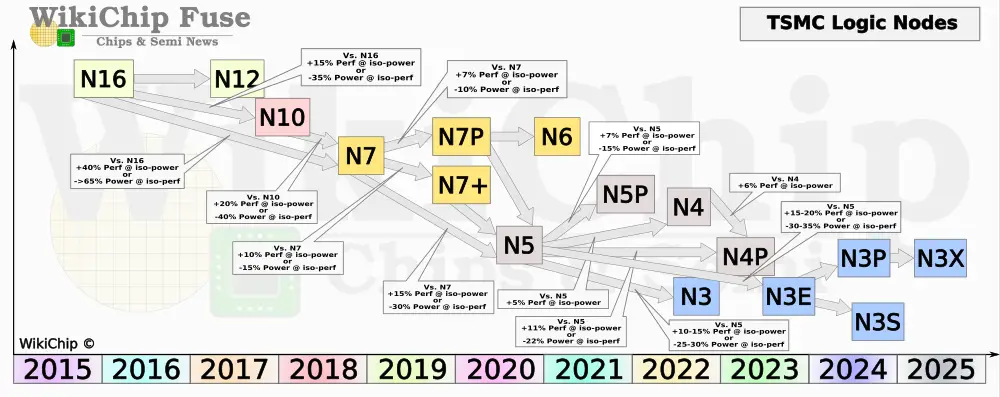
TSMC mentioned a number of additional variants derived from the N3E node – N3P, N3X, N3S, and N3RF.
TSMC plans to introduce a higher-density variant of the N3E node called N3S. This node is said to feature the highest-density devices for lower-power applications through library optimizations. The N3S is said to ramp around 2 quarters after N3E, placing it at around the mid-2024 timeframe.
Both N3P and N3X target high-performance applications similarly to N5/N4P and N4X. Their PPA and concrete timeline was not disclosed.
–
Spotted an error? Help us fix it! Simply select the problematic text and press Ctrl+Enter to notify us.
–

