
Intel Unveils Foveros Omni And Foveros Direct; Leveraging Hybrid Bonding
Today Intel held its global Intel Accelerated event where the company revealed a detailed process and packaging technology roadmap for the next half-decade. At the event, the company outlined some of its new packaging technologies.
This article is part of a series of articles covering Intel’s 2021 Accelerated Event:
- Intel 2021 Process Technology Update
- Intel Announces 20Å Node: RibbonFET Devices, PowerVia, 2024 Ramp
- Intel Unveils Foveros Omni And Foveros Direct; Leveraging Hybrid Bonding

EMIB Update
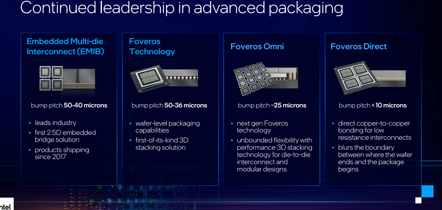
Intel has been shipping EMIB-based products since 2017. “Not only will Sapphire Rapids be the first Xeon product to ship in volume with EMIB, but EMIB enables Intel to build products that were impossible a couple of years ago. Indeed, Sapphire Rapids really is a big deal. It is the first theoretical reticle device delivering nearly the same performance as monolithic design in the industry. That’s a great achievement. Here again, EMIB is a great solution,” said Dr. Ann Kelleher, senior vice president and general manager of Technology Development.
Next-generation EMIB will scale from the current 55-μm micro bumps to 45-μm in next-generation EMIB. Third-generation EMIB will scale down to 40 μm.
| 1st Gen EMIB | 2nd Gen EMIB | 3rd Gen EMIB |
|---|---|---|
| 55 μm | 45 μm | 40 μm |
“We are also using that 45-micron pitch EMIB on a 92×92 mm package which will be the world’s largest ball grid array (BGA) package,” Kelleher added.
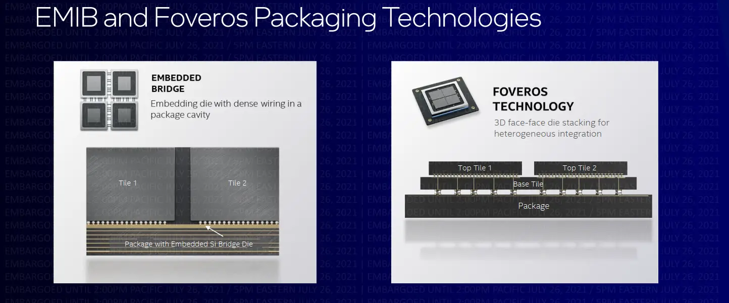
Foveros
Meteor Lake is Intel’s upcoming Intel 4-based product slated for 2023 for the client market. Meteor lake will make sure of Foveros Omni with a 36-micron micro bump pitch. The processor will make sure of multiple dies from different process nodes and will span from 5 W all the way to 125 W.

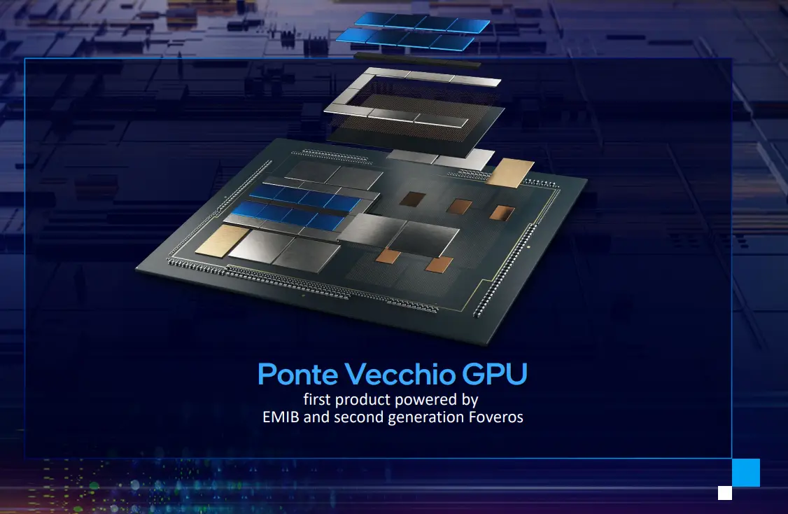
In addition to Metero Lake, Intel’s Ponte Vecchio GPU also utilizes second-generation Foveros technology.
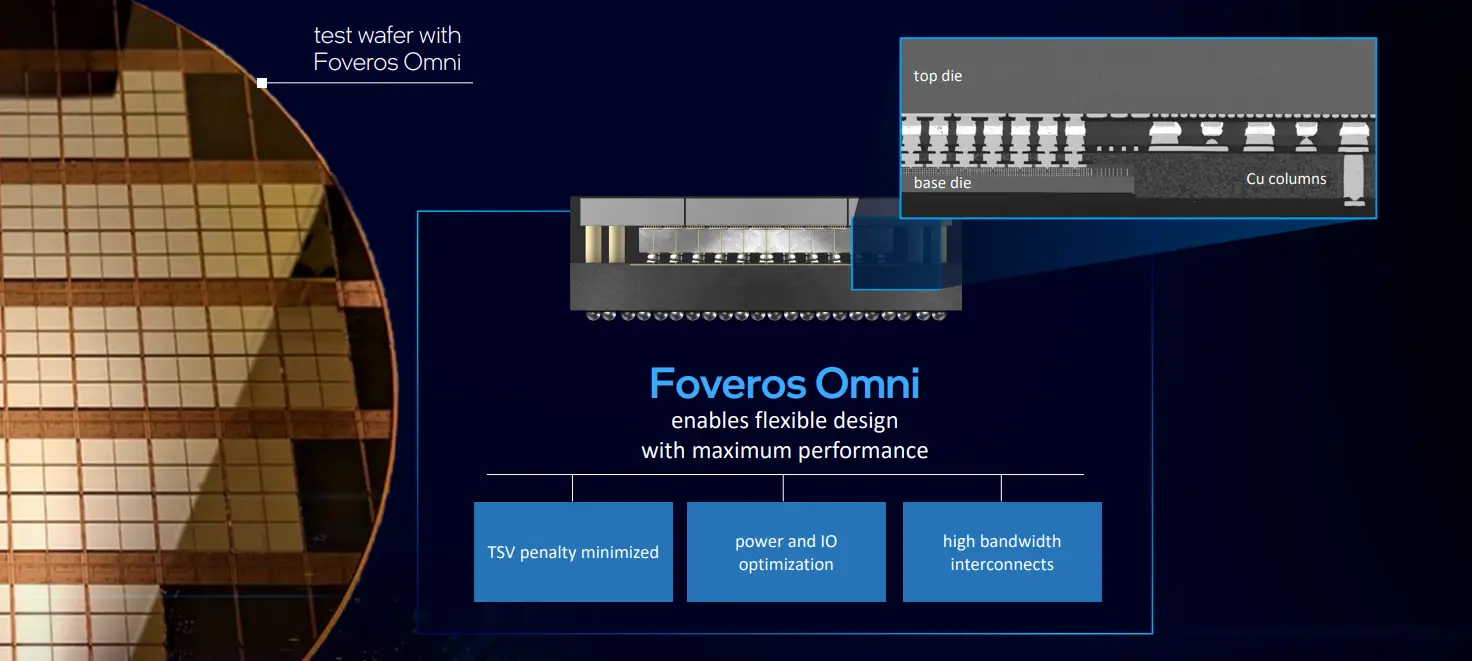
Foveros Omni
Foveros Omni is a new packaging technology Intel is introducing. In fact, the company already talked about this previously – Omni-Directional Interconnect (ODI) technology. Previously, the entire power delivery network, as well as signals all, needed to go through the TSVs to reach the top die. In Foveros Omni, copper columns are now introduced to directly feed power and signals to the top die, bypassing the TSVs. This offers a significant improvement to signal integrity and reduces TSV penality.
One of the other major changes to Foveros Omni is the ability to have multiple base dies. Previously multiple dies were only possible on top. Intel says that now multiple dies can be integrated as base dies and those dies can have different sizes as well as different process nodes.
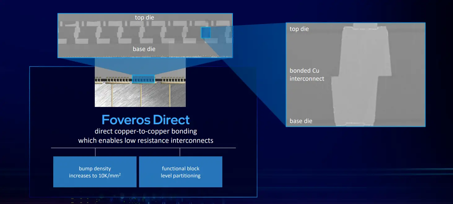
Foveros Direct
Foveros Direct is another new flavor of Foveros which is Intel’s implementation of Hybrid Bonding. Foveros Direct offers direct copper-to-copper bonding. It’s worth noting that Intel says it can mix and match Foveros Direct with other technologies such as Foveros Omni and even EMIB in order to create the best combination of technologies for a specific product of theirs.
Pitches
With each of the packaging technologies Intel disclosed, pitch scaling also continues. Foveros Direct currently offers 10-micron bump pitches which is a significant improvement even over Foveros Omni which offers 25-micron micro bumps. For Foveros Omni, this works out to around 1,600 wires/mm² at 0.15 pJ/bit. For Foveros Direct, this is increased to >10,000 wires/mm².
| 1st Gen Foveros | 2nd Gen Foveros | Foveros Omni | Foveros Direct |
|---|---|---|---|
| 55 μm | 45 μm | 25 μm | ≤ 10 μm |
–
Spotted an error? Help us fix it! Simply select the problematic text and press Ctrl+Enter to notify us.
–