
Intel Introduces Co-EMIB To Stitch Multiple 3D Die Stacks Together, Adds Omni-Directional Interconnects
Yesterday, ahead of SemiCon West, Intel held a small event for their packaging and assembly technologies. A number of engineering leaders from Intel’s Assembly/Test Technology Development (ATTD) and Components Research provided some essential insight into better understanding of the company’s IDM advantages in the area of advanced packaging. The company also disclosed a packaging roadmap and introduced a number of new technologies to complement their EMIB and Foveros.
Due to the short time between the event and when the announcement embargo lifted, this is a short article designed to give an initial high-level overview. We are working on a full in-depth article which will likely be published this weekend.
This article expands on Intel’s other recent disclosures:
Intel investor meeting series.
1. Intel Process Technology And Packaging Plans: 10nm in June, 7nm in 2021
2. Ice Lake Brings A New CPU, GPU, IPU, and I/Os, To Follow By Tiger Lake Next Year
Intel Architecture Day series.
1. Advanced 3D Packaging For More-than-Moore to Supplement 10- and 7-Nanometer Nodes
2. Intel Discloses 10nm Sunny Cove and Core Roadmap, Teases Ice Lake Chips
Co-EMIB
Over the last year, Intel has made a number of announcements concerning advanced packaging. EMIB is already shipping in a number of high-volume products such as Kaby Lake G and the Stratix 10 FPGAs and Foveros is expected to launch later this year with Lakefield. But the company is not stopping here. They are already talking about the next step – combining the two. One of the main technologies they disclosed is Co-EMIB.
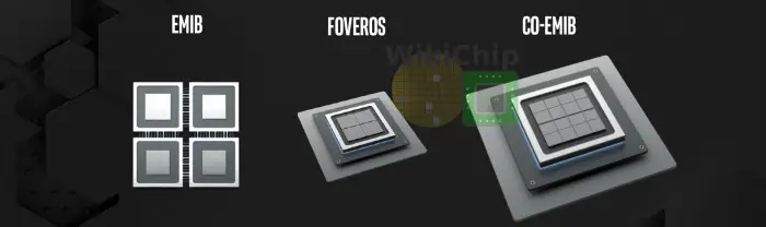
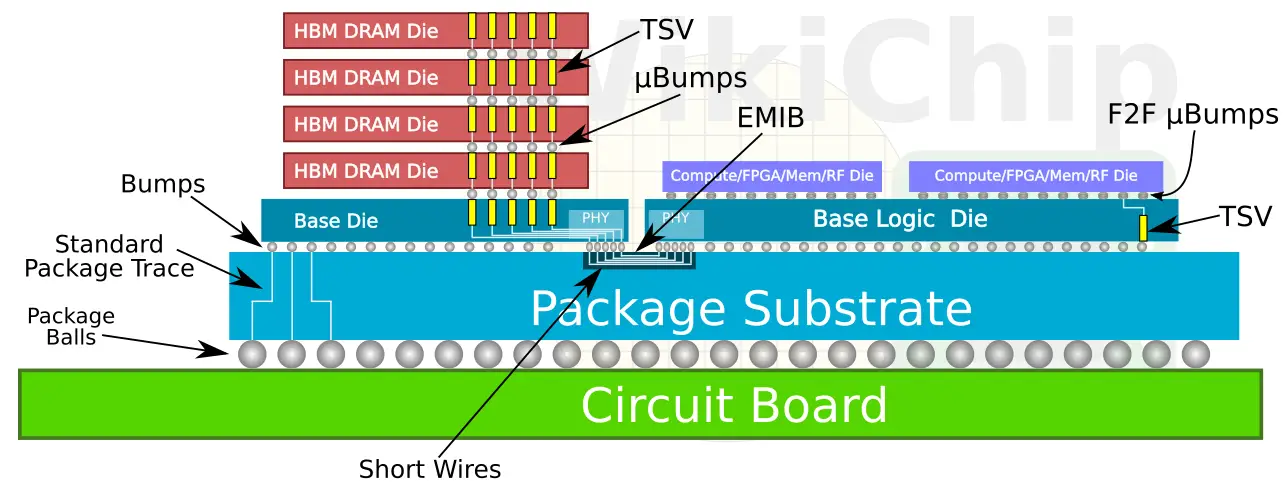
Under the Co-EMIB technology, Intel sets up an organic package with EMIB embedded in the substrate for the dies to sit on. They then take full Foveros stacks and whichever other dies might be used (e.g., HBM, transceivers, etc..) and flows them on the package. TSVs in the base die of the Foveros stack are exposed with tighter-pitched bumps for the EMIB. Co-EMIB allows them to build up bigger chips using smaller Foveros stacks or, alternatively, build up massive chips using reticle-size Foveros stacks in order to create chips that far exceed the reticle size.
Intel posted a small video illustration of how the process works. Again, we’ll have a full in-depth article later this week which will cover the full extent of the technology.
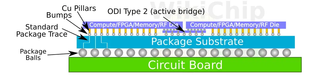
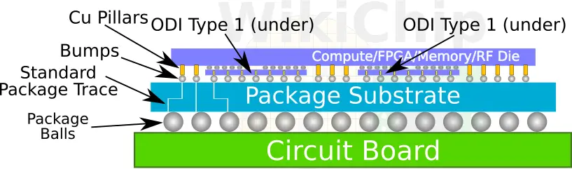
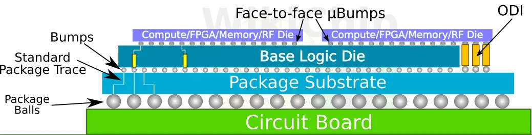
Omni-Directional Interconnect (ODI)
It turns out that Intel wasn’t done with Foveros either. Intel also announced a new technology called Omni-Directional Interconnect (ODI) which extends the idea of EMIB and chip stacking to actual dies in every direction – fully under, partially under die and serving as a bridge, and even hanging over. ODI comes in a number of configurations known as types. Under configuration Type 2, an active die can double up as EMIB between two dies. In many ways, it’s an active bridge, but not embedded in the substrate.
Under configuration Type 1, an active die is fully embedded under a bigger die. In this configuration, the copper pillars surround the die on all sides.
A third configuration, essentially a special case of Type 2 was also mentioned whereby a die hangs over the edge of a base die (or some other die underneath it) just slightly. In this configuration, the edge of the die is used for thicker power pillars.
Intel has a small video illustration of this technology as well.
–
Spotted an error? Help us fix it! Simply select the problematic text and press Ctrl+Enter to notify us.
–