
Intel Process Technology And Packaging Plans: 10nm in June, 7nm in 2021
Earlier this week Intel held an Investor Meeting. This is the first Intel Investor Meeting in over two years. Intel outlined its long-term process technology roadmap and plan of attack, including an update on their 10-nanometer node.
This article is part of a series that details Intel’s Investor Meeting.
1. Intel Process Technology And Packaging Plans: 10nm in June, 7nm in 2021
2. Ice Lake Brings A New CPU, GPU, IPU, and I/Os, To Follow By Tiger Lake Next Year
See also our series that details Intel’s Architecture Day.
1. Advanced 3D Packaging For More-than-Moore to Supplement 10- and 7-Nanometer Nodes
2. Intel Discloses 10nm Sunny Cove and Core Roadmap, Teases Ice Lake Chips
xPUs
Intel is gearing up to release a plethora of new architectures in additions to their traditional CPUs, including new GPUs, FPGAs, and NPUs. They have now lumped it together under the name xPU where the x can be substituted for any of those architectures. A little silly, but we’ll play along.
Process & Packaging
With the help of Moore’s Law, continuous integration of additional components onto a single die delivered better performance and brought costs down. With the difficulties the industry is facing on the leading edge of Moore’s Law in current nodes, a new paradigm shift has been installed. We have seen companies such as AMD and Huawei moving there first as a way of overcoming the massive challenging involved with yielding big dies. Intel’s shift to chiplets has been planned for quite some time now. It’s only now that we are slowly getting to see their plans.
Intel first disclosed their 3D packaging solution at Intel 2018 Architecture Day. We got a little bit more detail about their vision here. “Going forward, Intel is expanding the formula of integration well beyond the single die,” Renduchintala said.

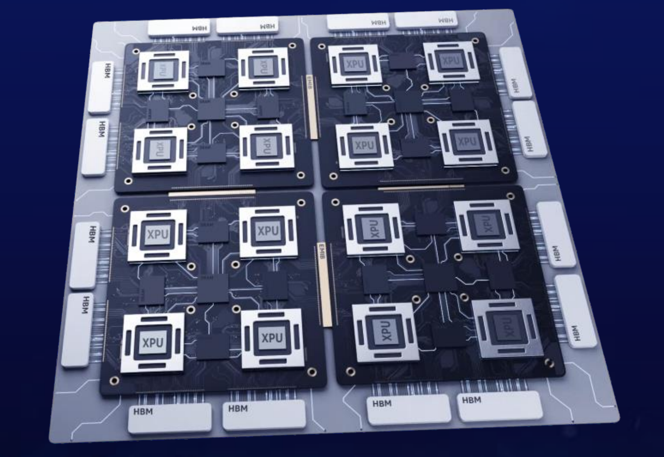
Compared to the single integrated circuit on the left, the product on the right consists of many xPUs on different process technologies optimized for their specific use-case. Those chips are then integrated onto a single package using 2D and 3D integration technologies such as EMIB and Foveros. For Intel, this means new technologies and capabilities can be developed independently and intercepted much earlier. Up to 2 years earlier according to Renduchintala. He added that compared to multi-chip packaging, “Foveros enables up to 10x increase in interconnect bandwidth while reducing the interconnect power by 6x at the same time.” One interesting remark made by Renduchintala is that this approach will allow Intel to selectively outsource various IPs that do help with product differentiation.
It’s difficult to know how much of the illustration shown is real and how much creative freedom was involved. If we were to scrutinize the drawing a little, we can see 4 chiplets sitting on some kind of interposer along with what appears to be four SRAM chips and another chip. There are four HBM stacks connected to each of those interposers. In total, there are four of those interposers interconnected using EMIBs for a total of 16 xPUs, 16 SRAM chips, 4 unknown chips, and 16 HBM stacks.
3D Lakefield
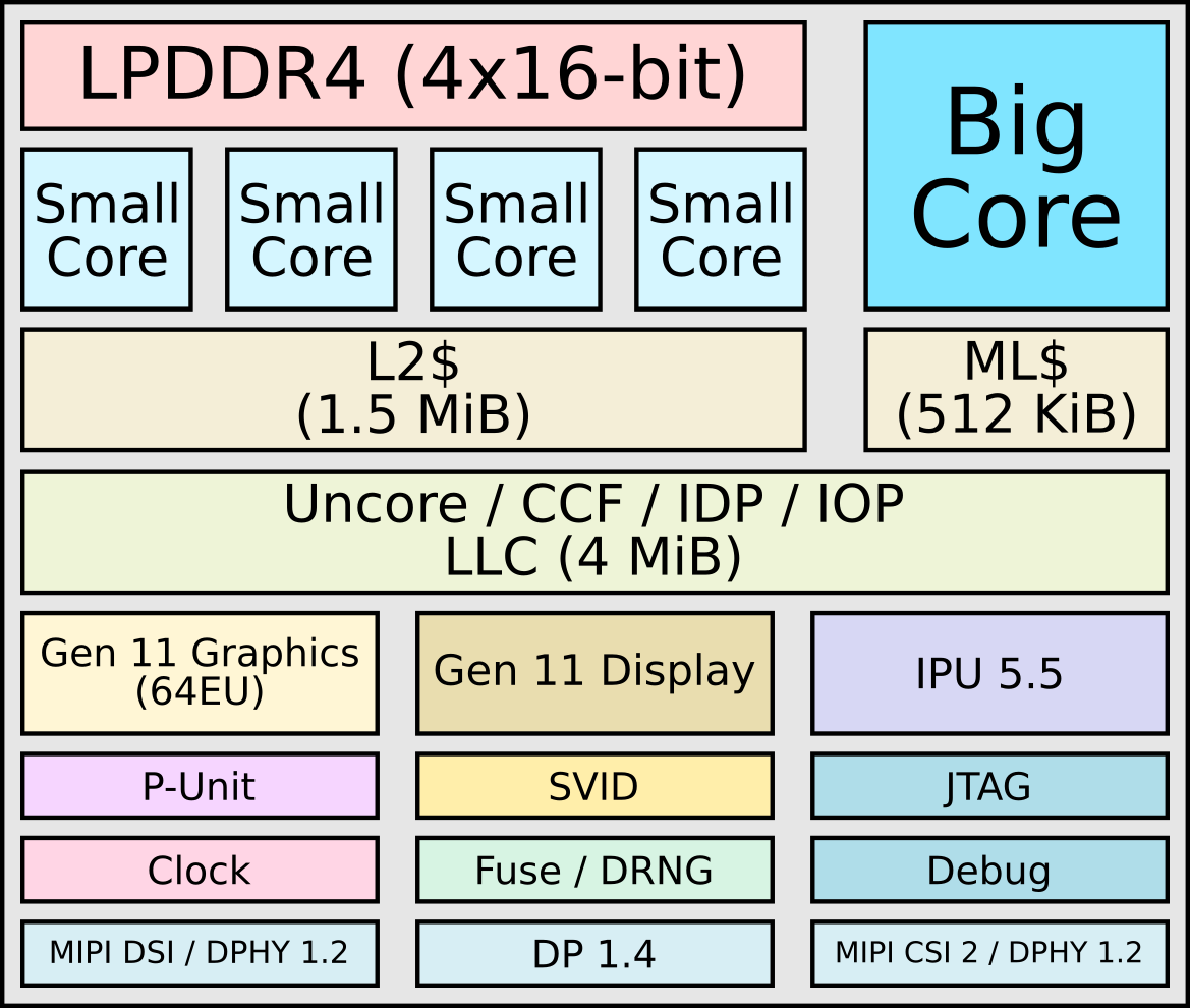
Lakefield is the first product that makes use of Intel’s advanced packaging technology. The chip was first conceptualized in 2016 with one of their largest customers for intelligent agents. The chip is a three-chip stacked solution including the DRAM on-package.
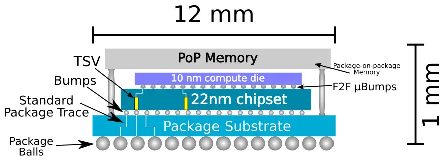
Lakefield’s main goals were: ultra-low power but high performance, always on, always connected, one-month standby, and smartphone-like form factor. The final design is a 12mm x 12mm x 1mm package. A base die is manufactured on Intel’s ultra-low leakage 22nm 22FFL process. It integrates the chipset and the always-on always-connection functionality as well as the power delivery subsystem. On top of the base die is the compute die. Manufactured on Intel’s 10-nanometer process, it houses the high-performance Sunny Cove core along with four lower power Tremont Cores.
“This combination enables Lakefield to achieve standby power of 2.6 mW and also burst to 27 Watts when high performance and demanding workloads are required. You couldn’t have done that in a monolithic-constrained environment,” said Renduchintala. At the top of the chip is a POP DRAM module.

Lakefield will be in production by the end of this year.
Lakefield is not a one-off product and the company is already working on a series of follow-up designs for the next couple of years.
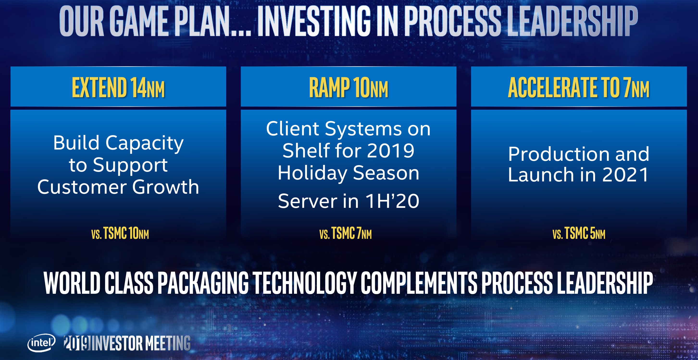
Concurrent Development of 3 Nodes
Intel CEO Bob Swan opened the event outlining their current investment. Currently, there are three leading-edge process technologies in development and in production. The company’s main node – 14 nm – remains in development being further improved for higher performance and lower power. With the current shortage situation, they have been working on building higher capacity which they say will be fully resolved by the fourth quarter of this year. Intel’s 10-nanometer process is finally ramping. Bob Swan reported that Ice Lake mobile chips will start shipping in just under four weeks with “products on shelves for the 2019 holiday season.” For clarification, this means the fourth quarter. Bob Swan stated that Ice Lake server CPUs will be a fast follow for the first half of 2020. Looking a little further out, the company’s 7-nanometers is also well under way. Swan expects “production launch of 7-nanometer products in 2021.”
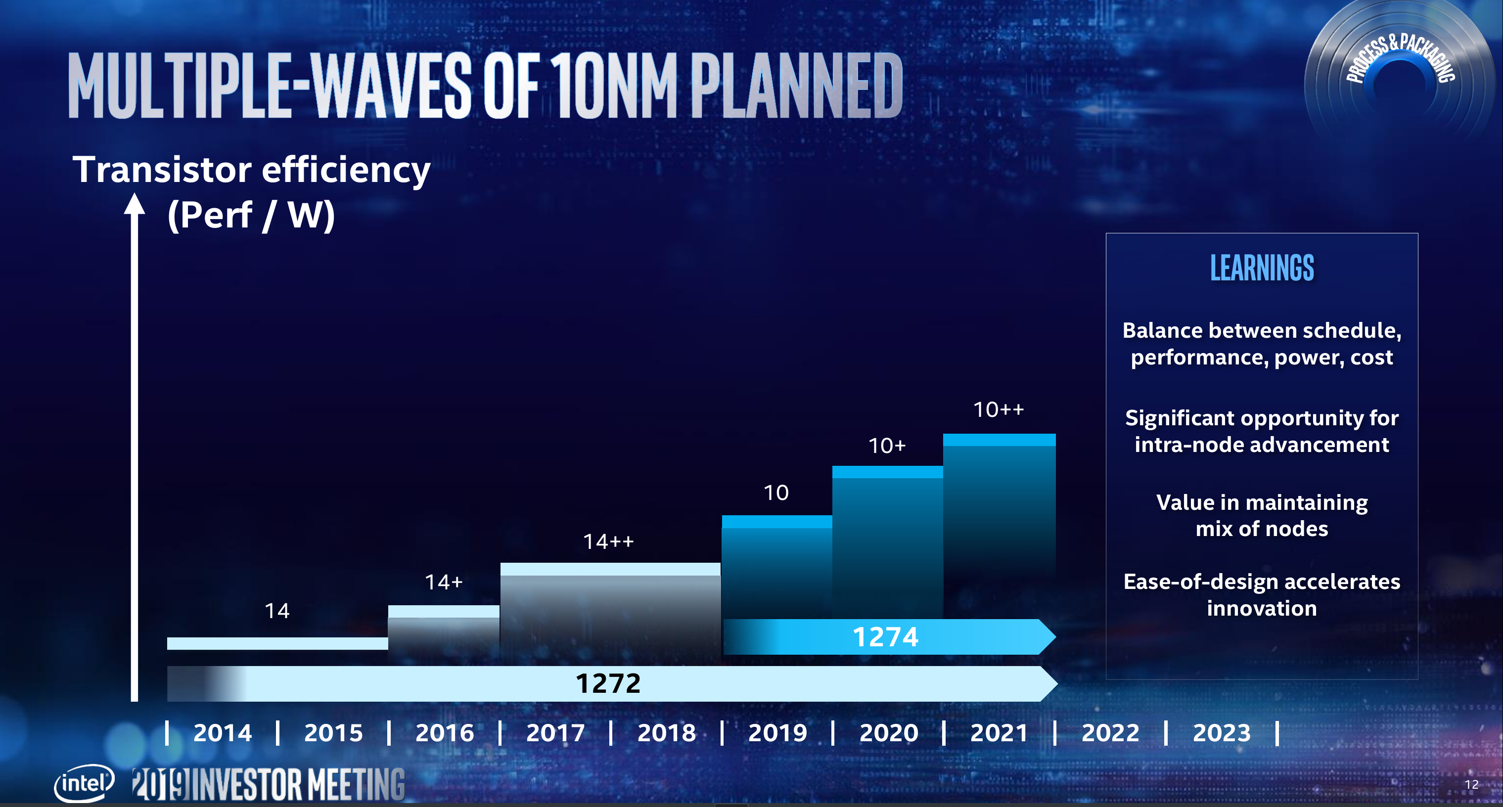
10 NM – We Messed Up
Murthy Renduchintala gave an update on their 10-nanometer. As we know, their 10-nanometers process is incredibly complex, involving unique standard cell designs, a large compaction ratio, cobalt interconnects, and made use of very complex lithography techniques such a SAQP on top of it all. Needless to say, the risk associated with each feature individually grows exponentially when combined. “To achieve this, the 10-nanometer team took on multiple revolutionary modules with inherit technical risk,” He said. “But in hindsight, that team took on way too much risk in one step. And the interplay of those revolutionary modules proved to be very challenging and the actual schedule for 10-nanometer is really a result of that risk profile playing out.”
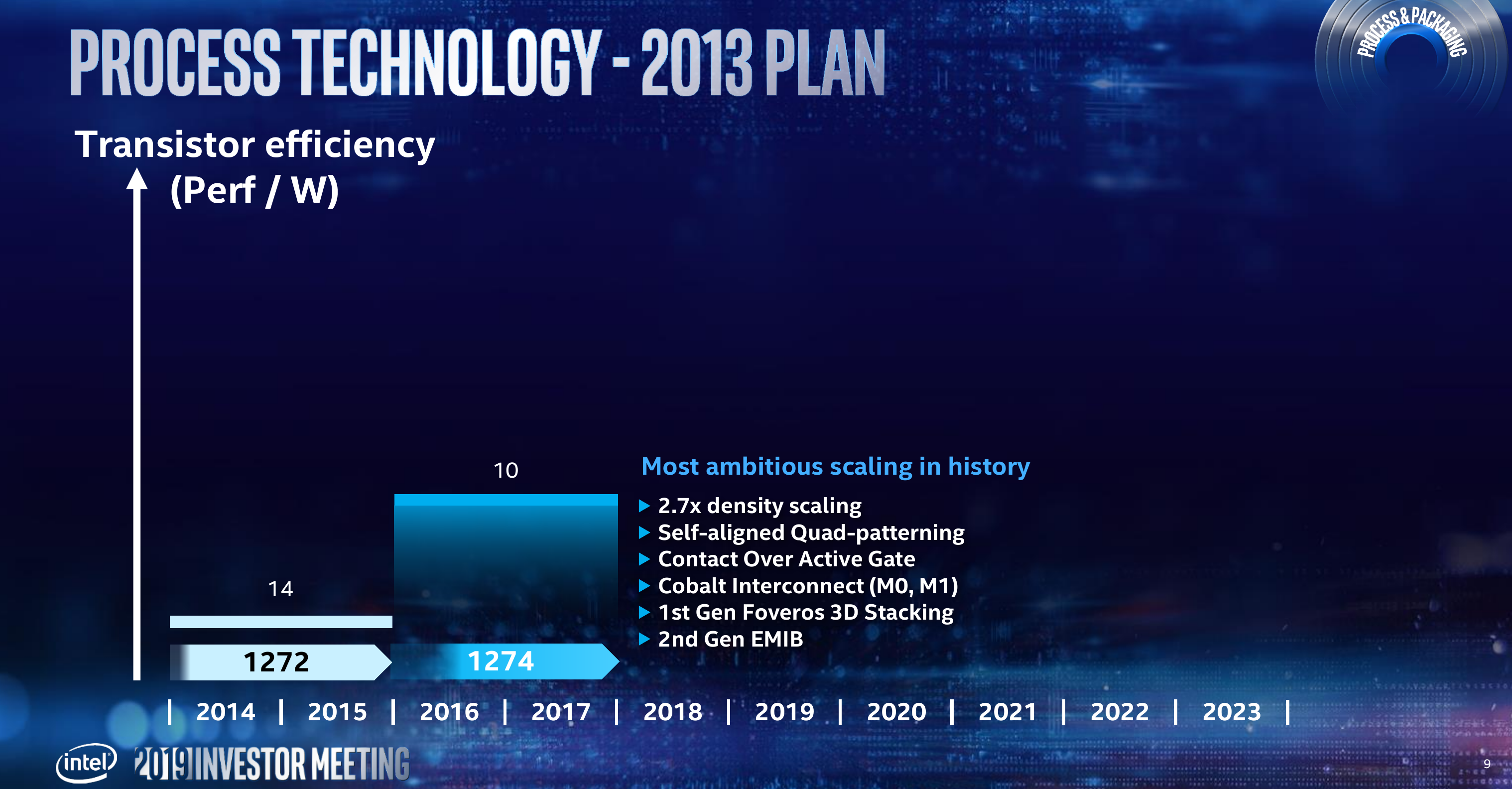
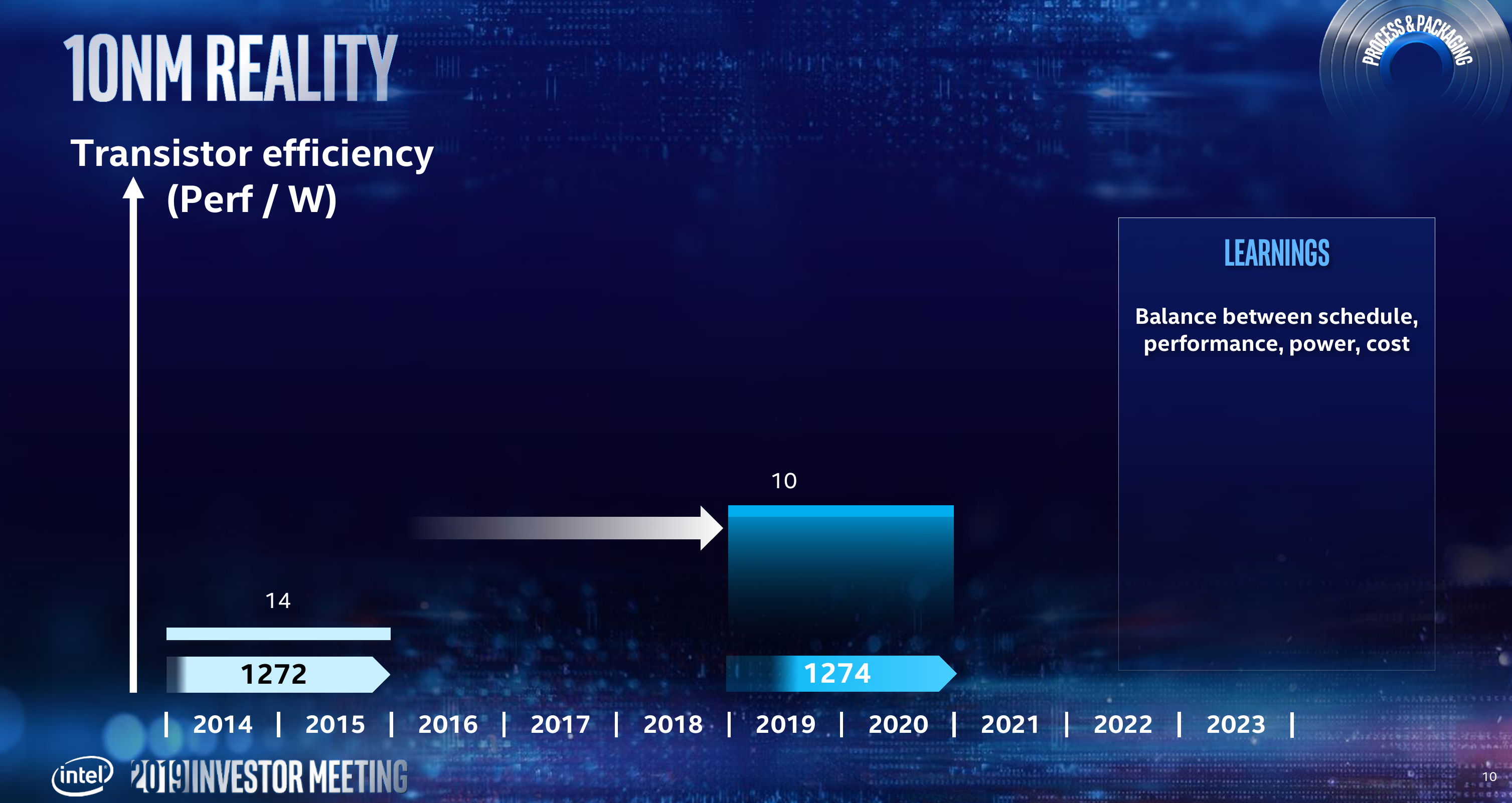
“We learned one clear lesson from that experience and that was the need to make sure that our engineers were given clear guidance on the balance of priorities between scaling and cost but also making sure schedule, power, and performance was taken into account when they define their technical plan of attack.” He added.
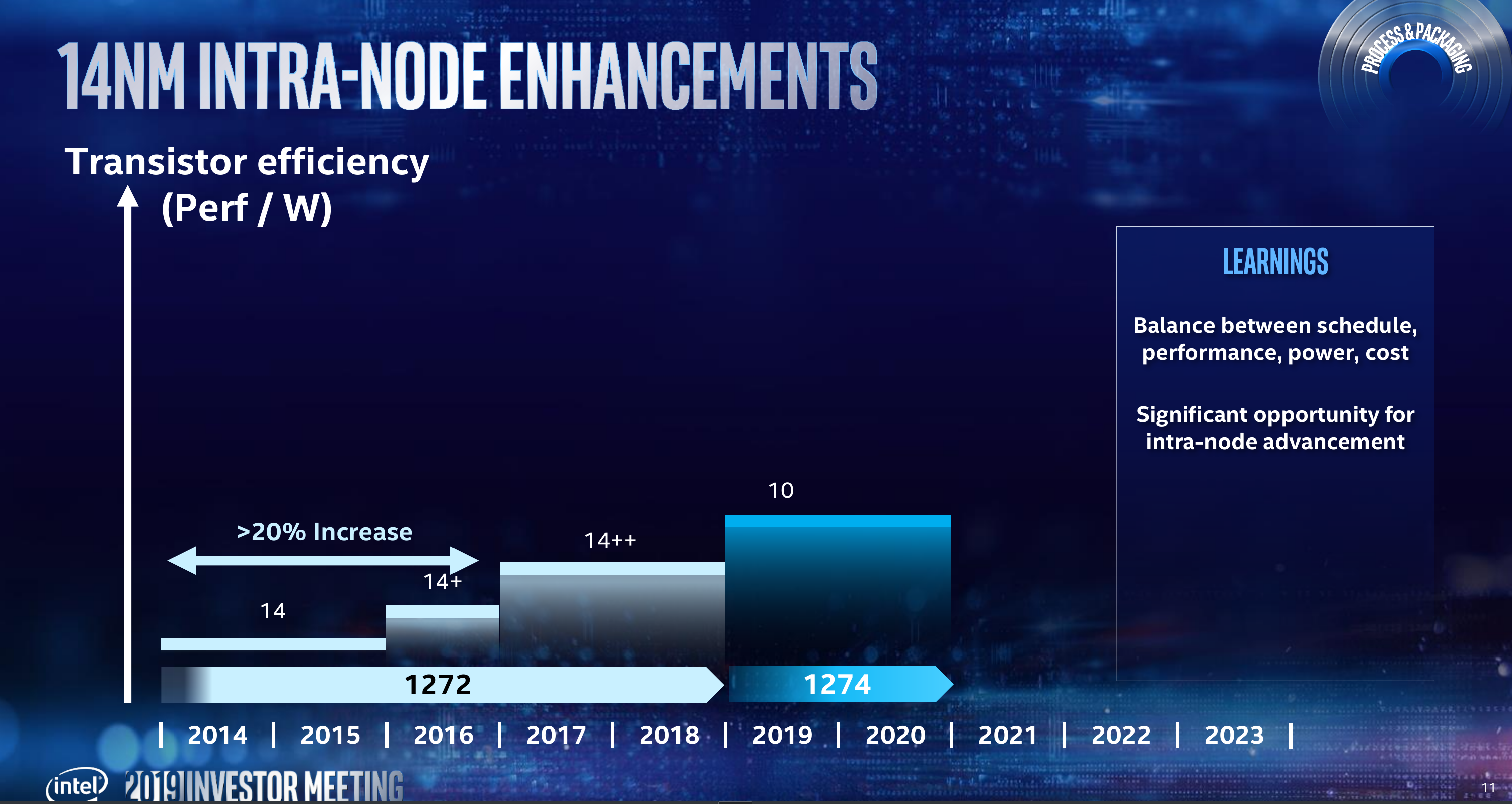
Filling the Void by Prolonging 14 NM
To fill the gap created by their 10-nanometer troubles the company introduced two iterations of their 14 nm process – 14nm+ and 14nm++. Renduchintala reported that compared to their first-generation 14nm node, Intel achieved a greater than 20% in transistor efficiency on 14nm++. The take from this is the value they can extract from inter-node optimizations and moving forward, all their future nodes will have planned inter-node optimizations.
10 NM
Intel also gave an update on their 10-nanometer node. 10 nm has gone into high-volume production at the beginning of the year. “We are delivering, without compromise, on the original performance and scaling targets,” said Renduchintala. Their first-generation 10-nanometer node will follow by two additional inter-node optimizations – 10nm+ and 10nm++ planned for this year through 2021. It’s worth noting that even after 10 ramps, Intel will continue to leverage their 14-nanometer node for mix applications such as cost-sensitive products and to speed various developments wherever it makes sense.
7-nanometer
“7-nanometer will be the fullest realization of our new approach,” said Renduchintala. Intel made schedule and time-to-market a priority and >15% improvement in transistor efficiency over 10 nm. With 7, Intel claims to have significantly reduced the design rules complexity of their process by 4x. This is important as it would more easily allow engineers to shift designs between the various internodes. As was expected, due to the feature sizes, 7-nanometer will make use of EUV. It will also feature the company’s next-generation packaging technology. Intel plans to introduce 7nm in 2021 and overlap it with the last node of 10nm++. It will be succeeded by at least two more iterations – 7nm+ and 7nm++ for 2022 and 2023.
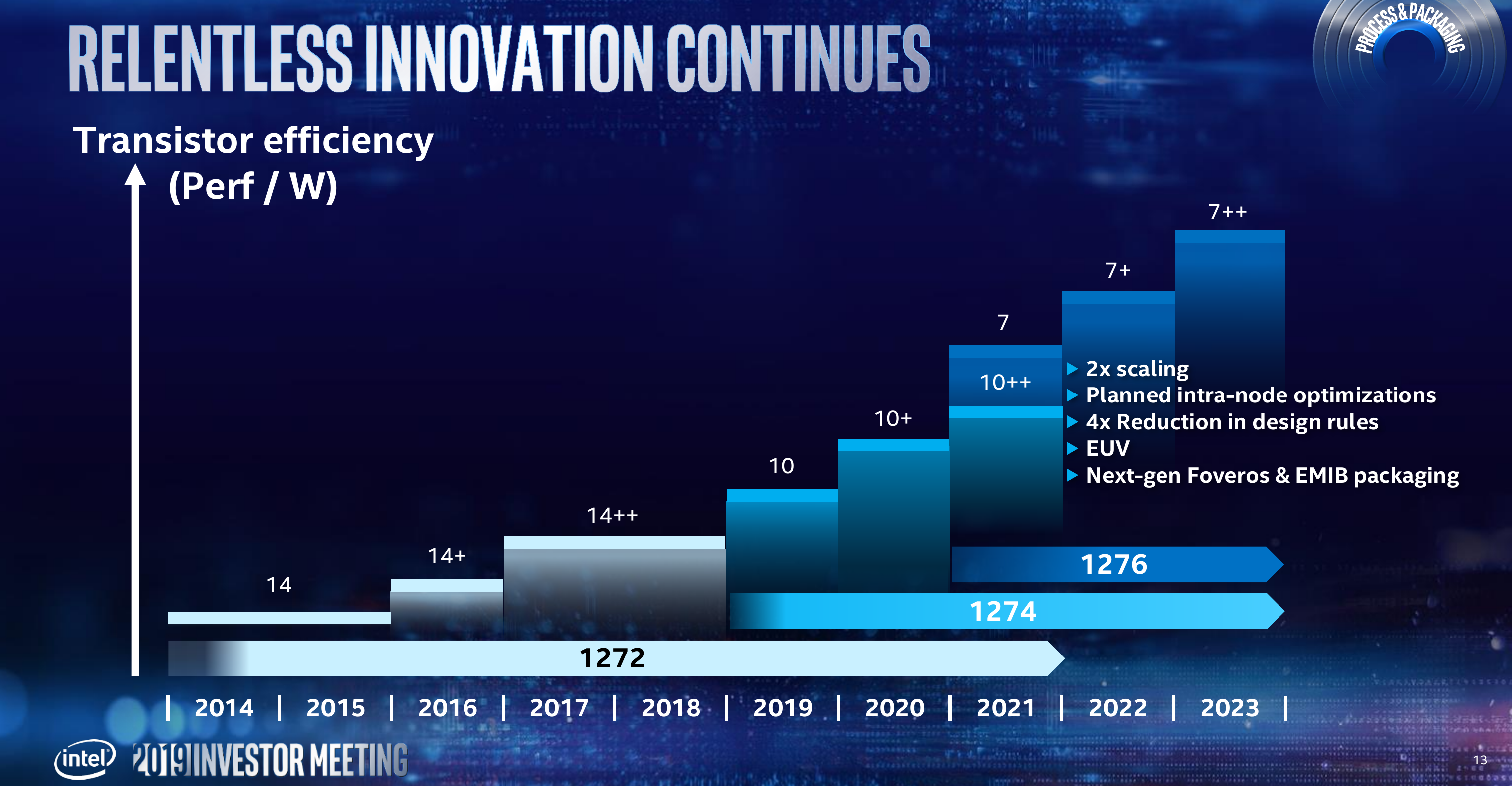
Their lead product for their 7-nanometer will be a general-purpose GPU for the data center and HPC. This GPU will also be powering Aurora. This is important because the success of the first exascale supercomputer in the United States now hinges entirely on perfect execution of Intel’s 7-nanometer team. Even a slight delay of just a quarter or two can potentially result in great humiliation for the company with the AMD-based Frontier exascale supercomputer beating them on the launch date.
We believe that for their 7-nanometer, Intel will make use of a high-mobility Ge/Si-channel FinFET transistor.
![]()
It’s worth noting that the slide indicated 7-nanometer having 2x the density of their 10-nanometer node. The slide contradicts the 2.4x target disclosed by Intel’s previous CEO, Brian Krzanich, during their 2018 Q1 earnings call. Based on communications we had with Intel following their event, it’s our understanding the today’s slide was more of a rounded estimate designed to demonstrate that the company is going back to their more traditional scaling compared to the aggressive scaling they took for their 10nm node. We believe that BK’s disclosed target of 2.4x, similar to their 14nm specs, is, in fact, the real compaction ratio.
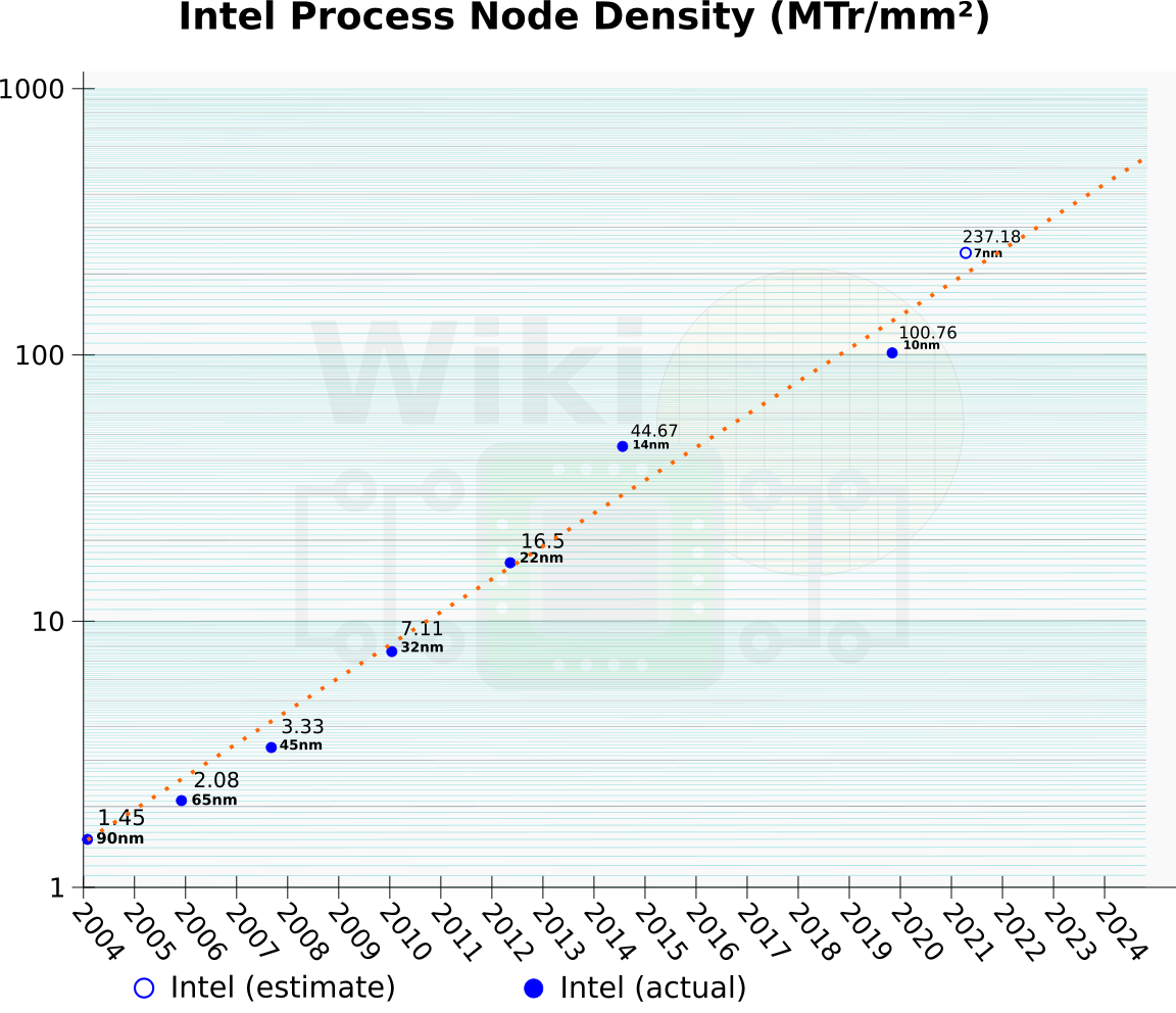
If Intel’s 7-nanometer node ramps as planned in 2021, we estimate it at around 237.18 MTr/mm², making it very competitive with foundry offerings. Intel says lessons were learned and 7-nanometer will be the real test of their execution.
–
Spotted an error? Help us fix it! Simply select the problematic text and press Ctrl+Enter to notify us.
–