
SEMICON West 2019: ASML EUV Update
At Semicon West last week ASML gave an update on current EUV systems as well as the 0.55 high-NA systems which are in development.
Anthony Yen is ASML’s VP and Head of Technology Development Centers Worldwide. We must have attended over a dozen of his presentations over the last two years at various conferences. His talks almost always opened the same way: “EUV is almost ready for HVM.†This time was different.
“EUV, as of now, is in HVM.â€
ASML earnings call took place earlier this week. They shipped seven more NXE:3400B systems for a total of 11 new systems this year. This brings the total number of EUV systems in the field to 50, albeit not all systems are considered HVM-capable. ASML expects seven more systems in the third quarter and twelve more by the fourth quarter for a total of 30 machines by the end of this year.
Main Module
When referring to the main module of the current 3300/3400 systems, there are a number of key components. You have the droplet generator where the tin droplets are generated from. Those droplets get zapped, generating EUV light which gets directed to the intermediate focus.
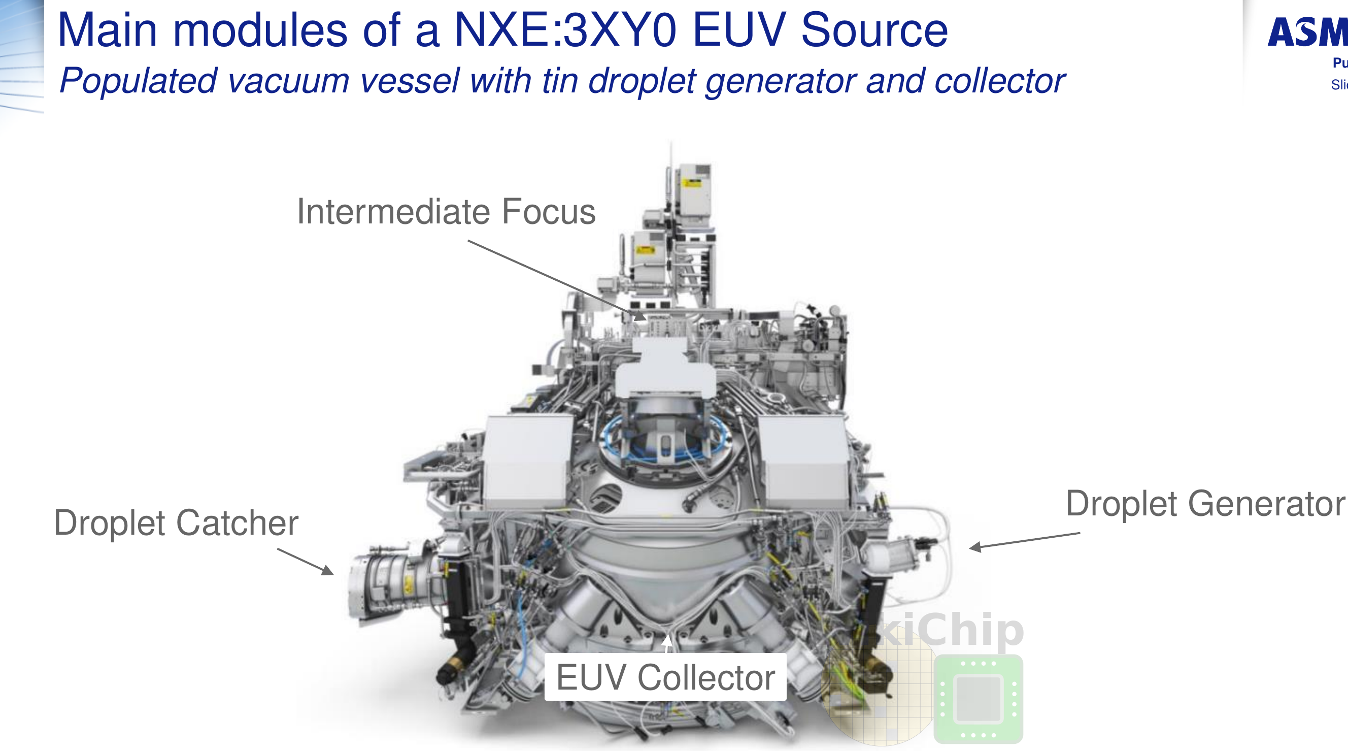
From this, we can highlight some of the key factors that affect the system uptime and power. In order to improve the system, you need a high input CO2 laser. This laser then zaps the tin droplets. When this happens, you need a high conversion efficiency along with high collection efficiency. This is done through the ellipsoidal EUV collector mirror. There are two foci here, the first one is when the tin is zapped which is then refocused at the second focus. Finally, droplets that failed to get zapped are then collected by the droplet catcher. Therefore, increasing efficiency and lowering dosage overhead is the name of the game.
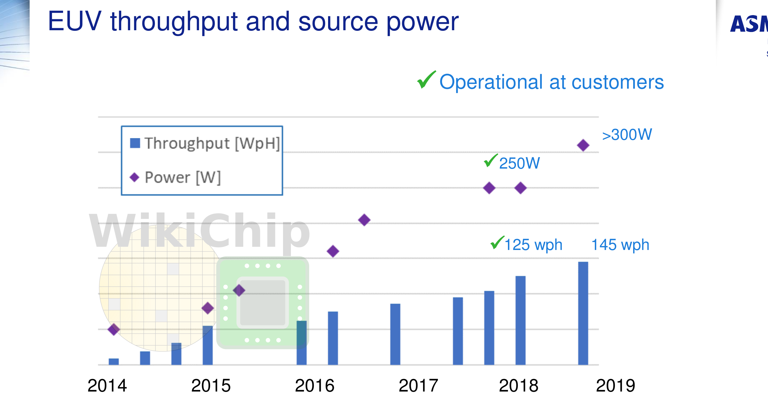
At their lab, Yen is reporting that ASML has achieved over 300 Watts for the source power. Currently, the source power installed at customers site remains 250 W. With 250 W, customers are achieving a maximum throughput of around 155 wafers per hour. Those numbers were corroborated by Britt Turkot from Intel earlier this year at the 2019 EUVL Workshop.
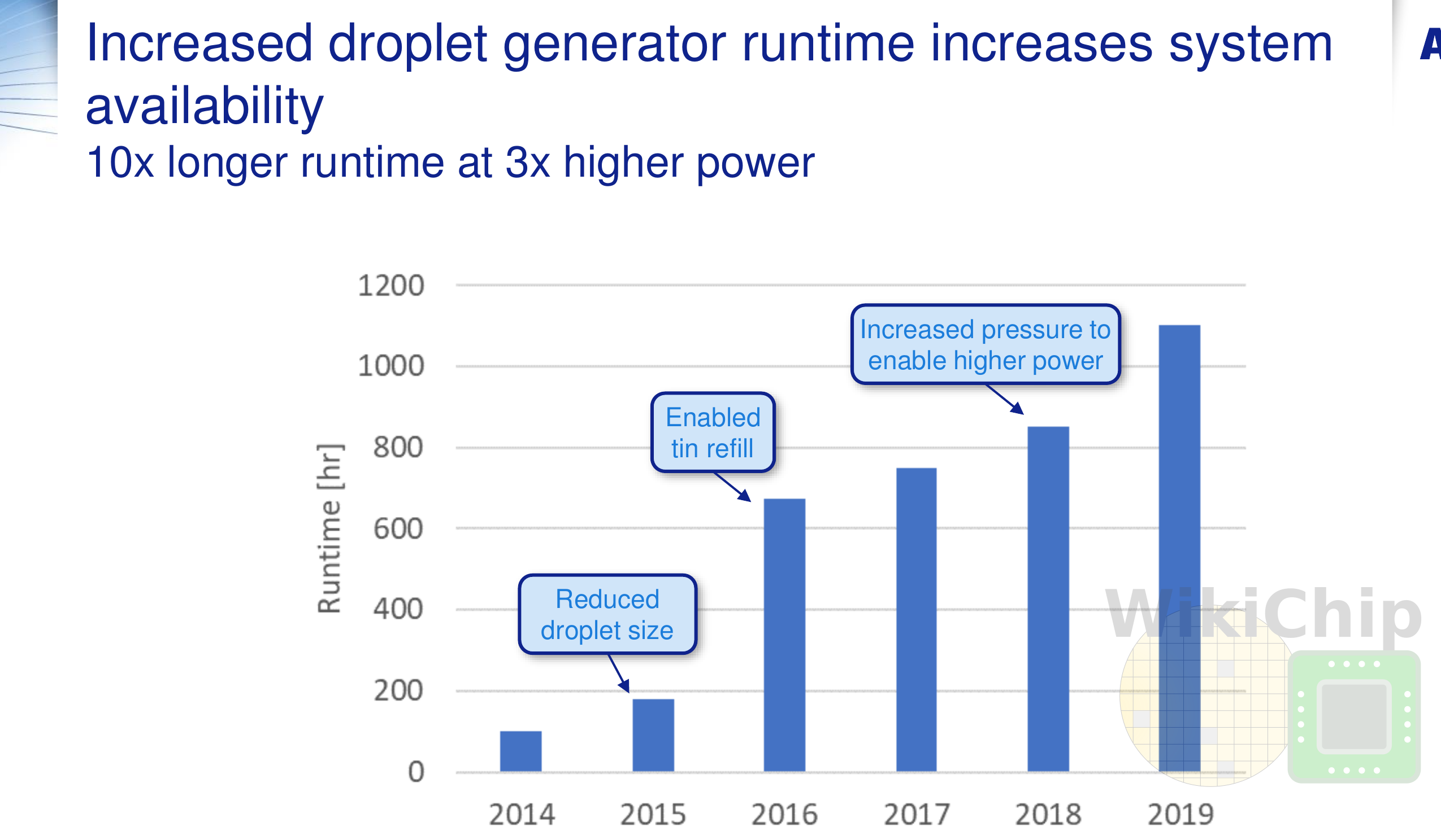
One of the components that impede system availability was the droplet generator. ASML is reporting that since 2014, the droplet generator has gone from around 100 hours in 2014 to over 1000 hours in 2019. Since last year, they have improved the lifetime of the droplet generator by 30 percent. It’s worth noting that there are other areas of improvement that can be made here. There is additional downtime involved in refilling the tin canister. As you will see later on, this will get addressed later this year.
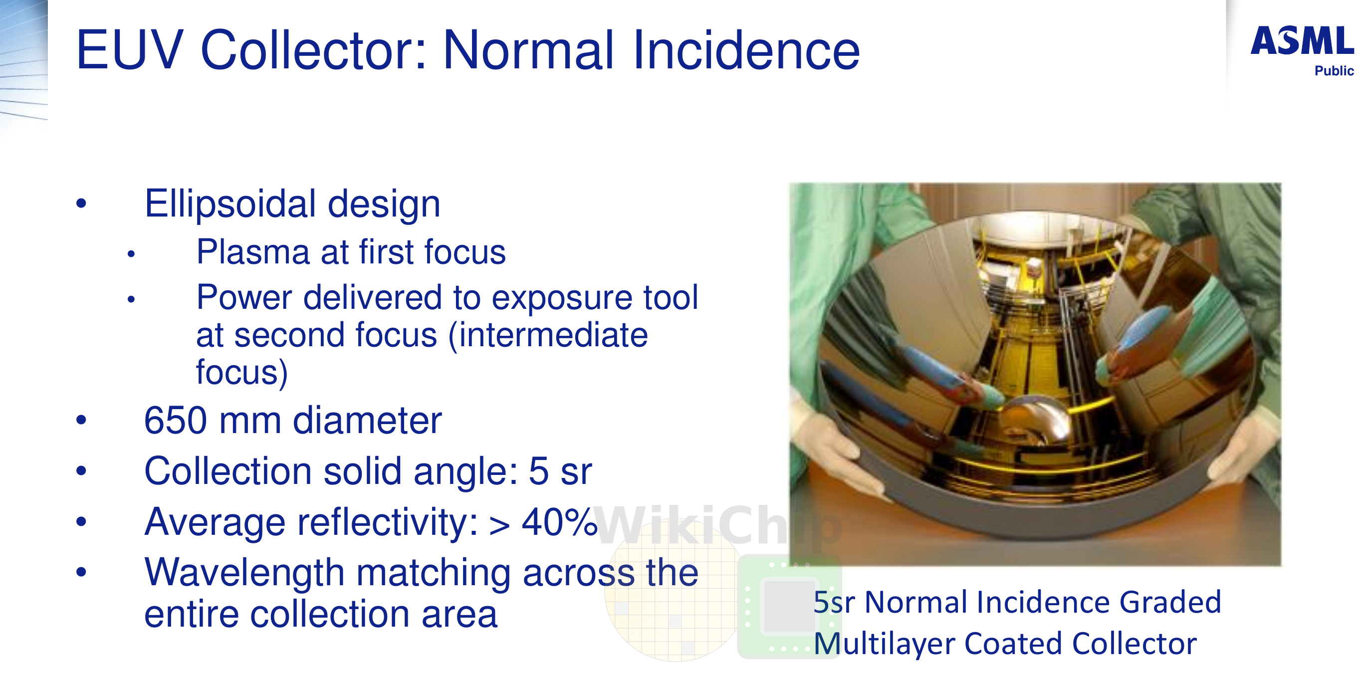
Another area of concern is the collector itself. This is a 650 mm diameter multi-layer graded mirror designed to maximize reflexivity. The critical issue here is how to keep it as clean as possible, preventing it from fogging up or getting contaminated. With their current customer installed NXE:3400B systems, Yen is reporting a degradation rate of around 0.15% per giga-pulse. ASML would like to get it down to less than 0.1%/GP at the same power (250 W). So they are within reach of this goal.
Today, the collector follows a fairly predictable lifetime which is degraded at the roughly linear trend. Once the collector is degraded enough, it needs to be swapped. This is a problem onto itself. A few years ago this would have taken as much as a week. Today, it takes a little over a day. ASML intends on reducing this down to less than eight hours with their next-generation NXE:3400C.
All of those improvements result in around a 70% availability for the bottom 20 percentile of the systems with top 20 percentile closing on 85% availability. Their goal is to exceed 95% availability which is where all DUV machines are today.
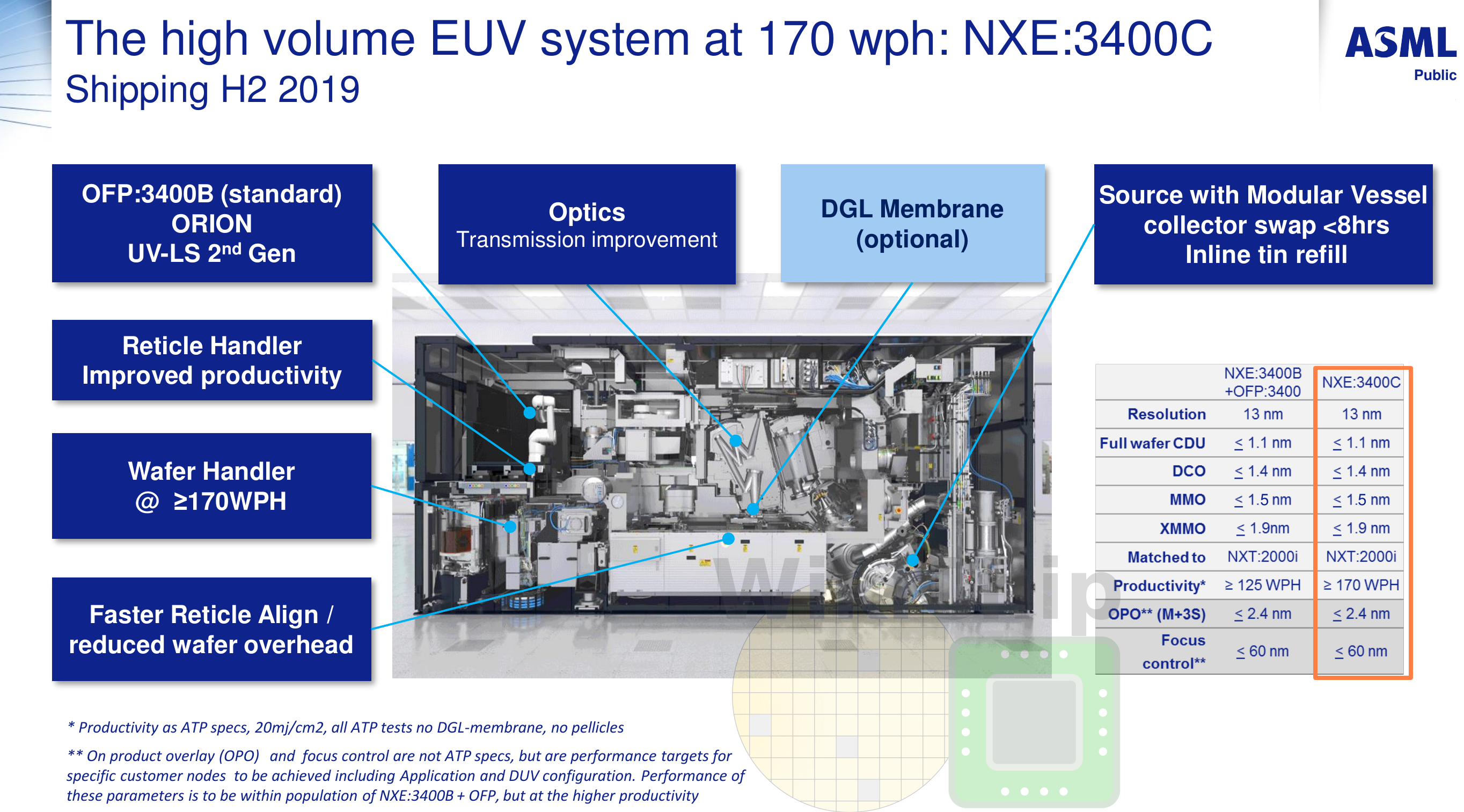
NXE:3400C
In the second half of this year, ASML will start shipping their next-generation EUV system. The NXE:3400C is an evolutionary tool intended to further address some of the deficiencies that were described earlier. This system is rated for 175 WPH at 20 mJ/cm². At the Q2 earnings call, ASML reported having the system running in the lab at 175 WPH, achieving 2000 WPD, operating at identical memory production conditions as their customer.
One of the special features of the new system is the modular vessel which has been redesigned for easier maintenance. Yen says that they are hoping that swapping of the collector can be reduced from just over a day to less than eight hours with this system. Additionally, they have changed the droplet generator refilling procedure. It no longers requires powering the system down in order to refill the canister and then bring the system back online. Refilling with the new system can now be done inline. All in all, with the combination of all those changes, they are hoping to reach the target 95% availability.
EUV Pellicle
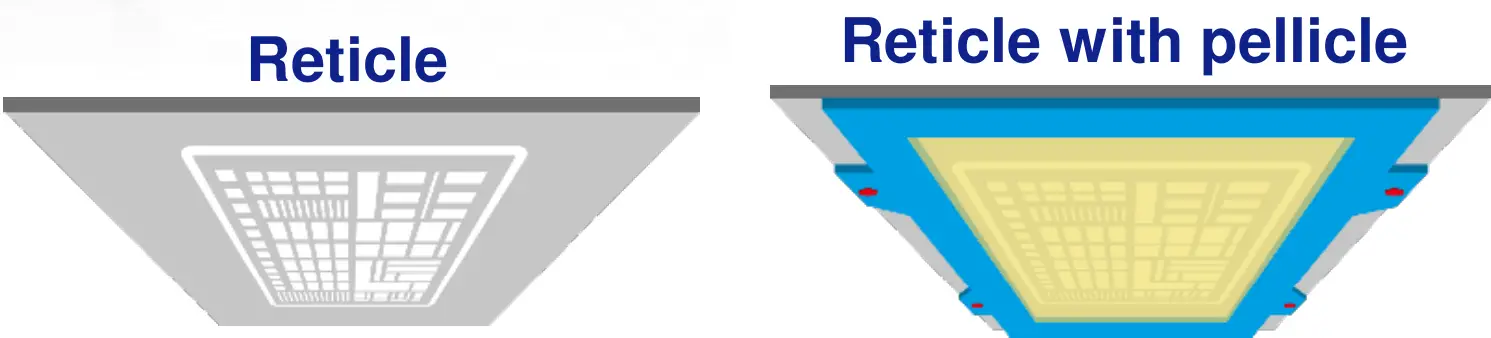
Another issue with EUV is front-side defects brought about by particles. Yen is reporting that when it comes to reticle area cleanliness, they are approaching 1 particle per 10,000 exposures.
For customers that cannot tolerate even 1 particle per 10,000 exposures, there is the option of an EUV pellicle. This is an ultra-thin transparent membrane that covers the mask and is intended to prevent particles from reaching the mask. While this helps with defects, the problem with using pellicles today is the degradation of light transmissivity. When some of the EUV is absorbed by the pellicle, it translates to a loss of power. Progress on this front has been extremely slow. In the last year and a half, the average transmissivity has only improved by around 3.5% to 83%. A good target is over 90-93% transmissivity but it’s unclear how the industry is getting there.
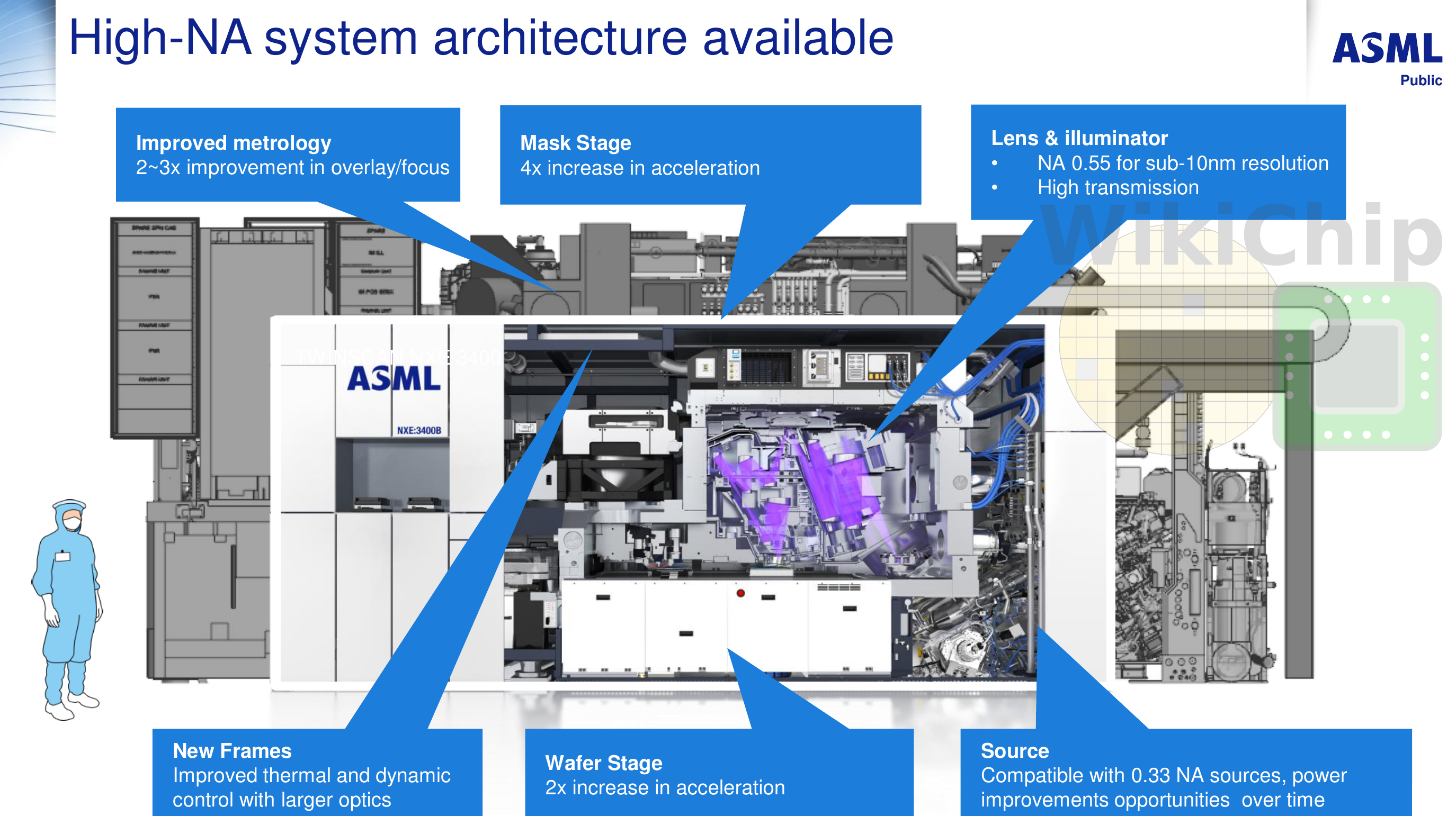
High-NA systems
Looking a little further, ASML already started working a high-NA system. The first system is not expected to ship until the end of 2021. The High-NA system is considerably bigger and heavier than the current 3400 systems. This machine uses a distinctly different lens system which uses a 0.55 NA anamorphic lens. These lenses are rated for 8nm half-pitch and give 4x magnification in the x-direction and 8x in the y-direction. Due to the lens which half the field, this system adds a few additional stages designed to increase acceleration.
One thing that doesn’t change with the High-NA system is the source which remains compatible with the 3400 systems. It’s worth pointing out that the source is actually situated more horizontal in the high-NA system compared to what it is now which will allow them to remove a mirror. The effect is similar to increasing the power by over 30%.
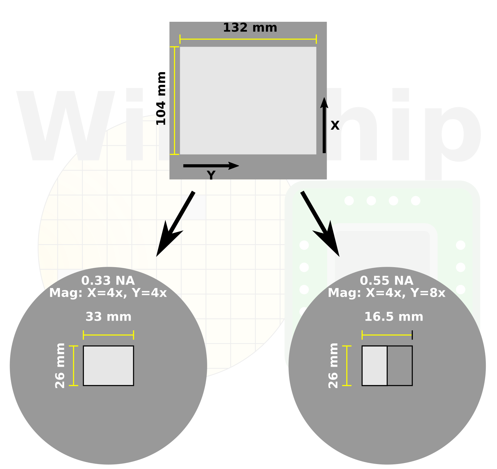
The increase in the lens magnification is done in order to reduce the shadowing effect. However, the impact of a 4x/8 1:2 magnification ratio is on the circuit design itself. With a standard 6†photomask, on the standard 0.33 NA machine, you get 4x/4x reticle which means a full field of 33 mm by 26 mm for a maximum die size of 858 mm². With 0.55 NA with anamorphic optics, you are looking at 8x in the y-direction, so your field is now halved. For circuit designers, this means an effective field of 16.5 mm by 26 mm for a new maximum die size of 429 mm². Say goodbye to the massive dies we got used to from Intel and Nvidia. Of course, this has been known for a long time now which is why advanced packaging has been such an important topic. By the way, with an effective field which is now halved, you take a hit to the throughput. This is somewhat addressed with 2x wafer stage acceleration while doing twice as many scans.
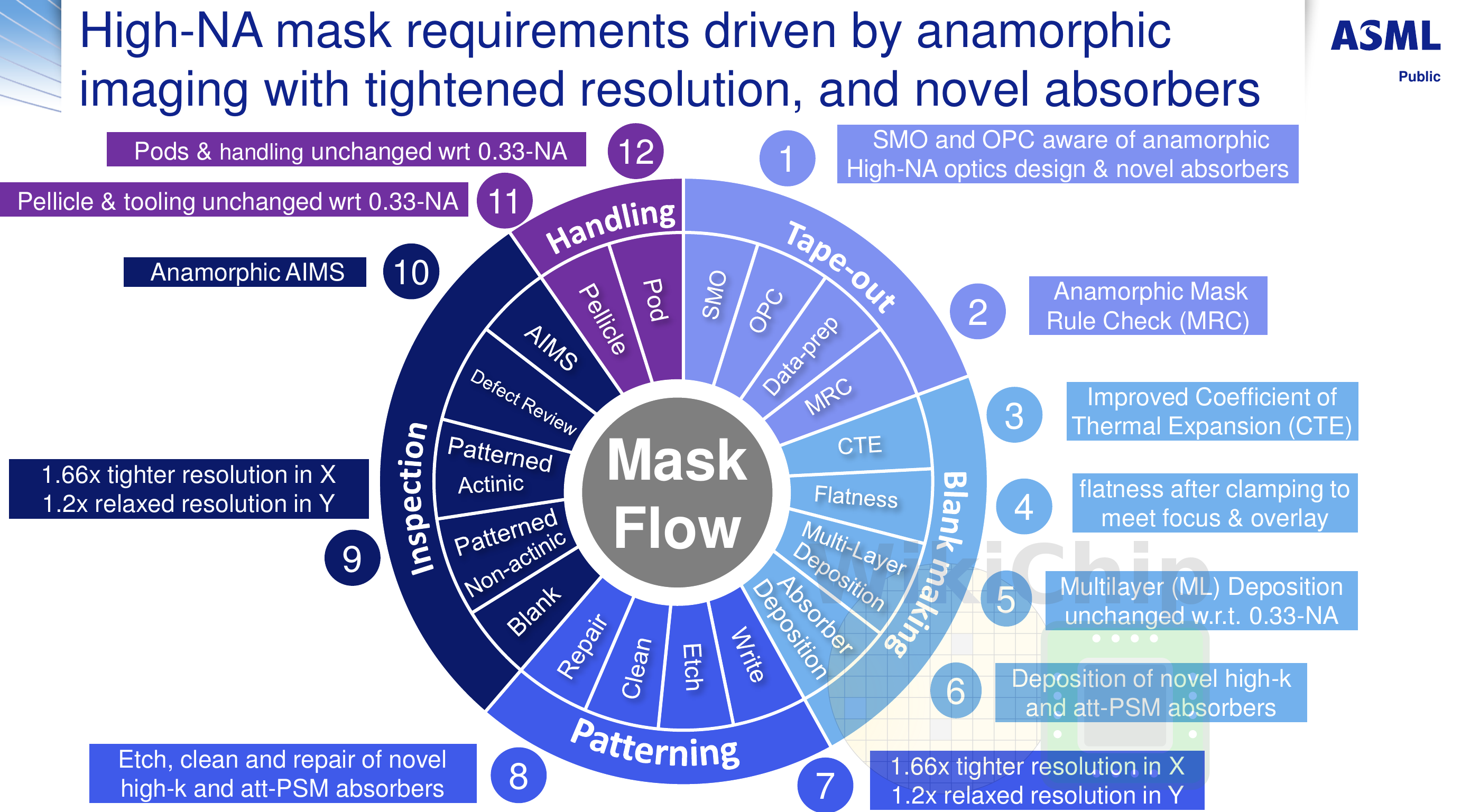
Ongoing Infrastructure Development – High-NA Masks And Resists
Currently, there remain a number of major infrastructure-related challenges. The mask infrastructure for High-NA is not there yet. The slide below lists some of the major requirements in all areas of the mask flow that must be taken care of.
One notable issue is the mask 3D effect which was talked about earlier. It requires new novel absorbers in order to minimize the problem. When a chip designer completes an IC design, the design is transferred from a file into a photomask. This mask serves as a master template from which the scanner can effectively print many copies of the IC by printing the pattern on a wafer. Traditionally, this was done by projecting light through the mask. The process works much like a typical overhead projector, except backward (going from a large image to a small one). For EUV, the mask is quite different. Here, the mask is actually based on the mirror-type mask blank. The different circuit patterns are ‘drawn’ on the mask through the use of absorber material along with an anti-reflective coating (ARC). The absorber material and the ARC sit on top of the mirror in a 3D-like structure.
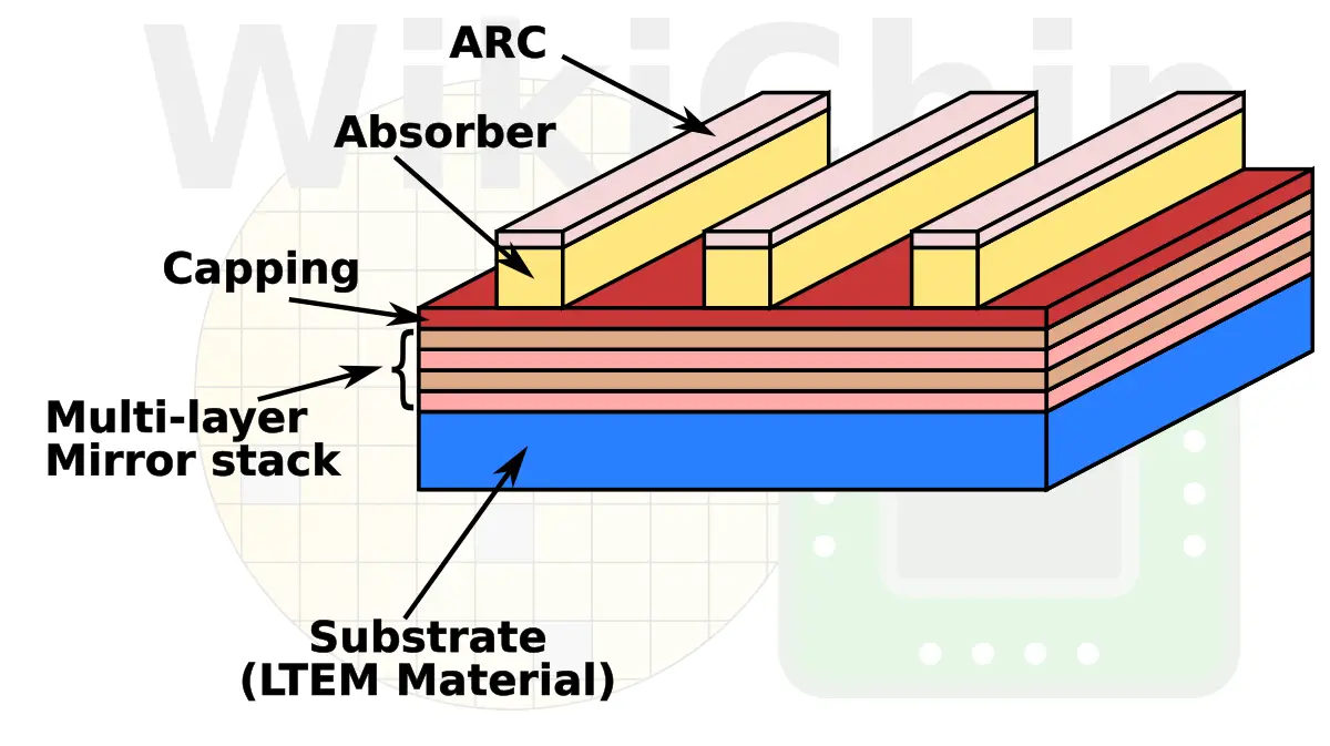
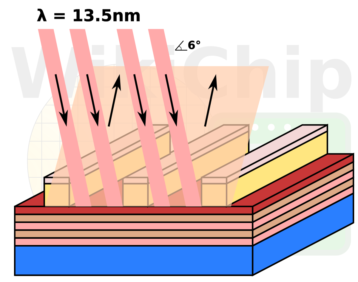
During operation, when light hits the mask (usually at a slight angle, around 6 degrees), sometimes the reflections from those structures can cause shadowing effects and aberrations.
Though the problem has been known for a long time, R&D has mainly been preoccupied with other aspects of EUV such as the main module and power source. Additionally, the effects are not too problematic at the 7-nanometer node either. However, heading down to the 5-nanometer and 3-nanometer, the mask 3D effects will become more pronounced.
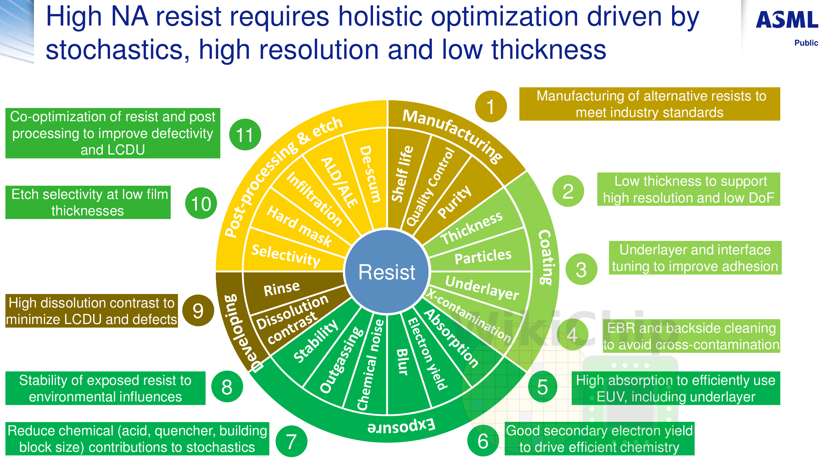
The photoresist side is in the same boat as the High-NA mask. There is a lot that has to be done.
 |
 |
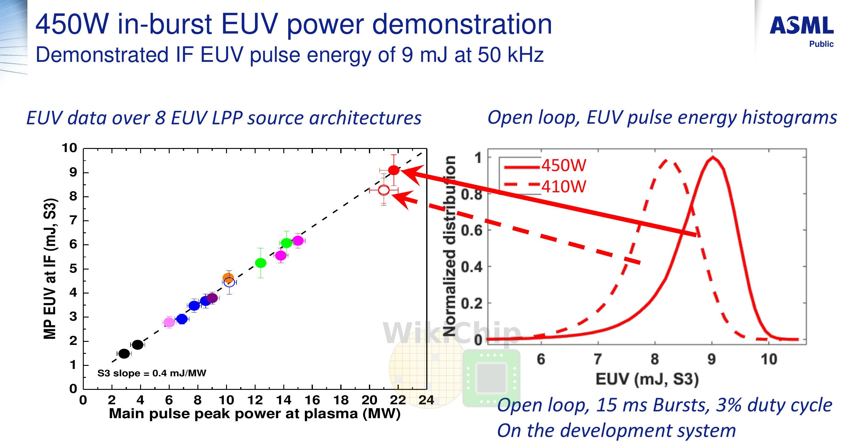
500 W Power For High-NA Systems
Looking a little further. Yen said that, at their San Diego lab, ASML has managed to reach 450 W of power. “By the time our High-NA scanners come out, I am sure we will be beyond 500 W,†he added. Around 500 W is about where ASML needs to be to reach 150 WPH at 60 mJ/cm² on their High-NA half-field scanners.
–
Spotted an error? Help us fix it! Simply select the problematic text and press Ctrl+Enter to notify us.
–