
A Look at Cerebras Wafer-Scale Engine: Half Square Foot Silicon Chip
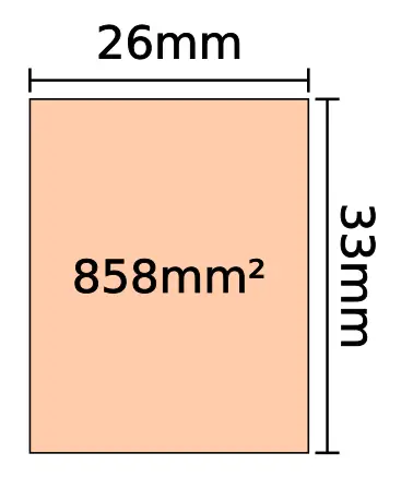
One of the major driving forces of Moore’s Law has been the need for the ever-increasing levels of circuit integration. There are generally two ways of increasing density – utilize smaller feature sizes (and layouts) or use larger substrates. Recent chips by companies such as Intel, IBM, and Nvidia often get close to the largest die possible on recent leading-edge nodes. Modern i193 and EUV lithography steppers have a maximum field size of 26 mm by 33 mm or 858 mm².
Making conventional dies that are any bigger in a monolithic way (i.e., non-stitching) requires new tools. There are, however, a couple of alternative methods. Wafer-scale integration (WSI) refers to the fabrication of monolithic chips that are – or nearly – as large as the maximum diameter of the wafer itself. WSI is not a new concept. The idea dates back almost half a century. Perhaps the most notable attempt was that of Trilogy Systems, an early 1980s startup cofounded by Gene Amdahl that attempted to design a high-speed computer using ECL-based wafer-scale modules. They came up with a wafer-scale ‘supercomputer’ on a 100 mm wafer for a chip the size of 6 cm². Trilogy Systems eventually succumbed to the economic reality of wafer-scale lithography of its time and by 1984 the company abandoned its effort. In 1989, Anamartic, a UK-based company announced its Wafer Stack. The Wafer Stack came with 20 to 160 MiB of memory using up to eight stacks of 150 mm wafers with each wafer integrating 202 1 Mib memory dies.
It has been over thirty-five years since Trilogy abandoned its effort and the semiconductor industry has undergone dozens of node transitions, four wafer size transitions, and significant gain in knowledge and experience of process technology that enables millions of transistors to be fabricated on every single millimeter of silicon with yields that would not have been imagined several decades ago. So maybe it’s time to give it a serious second chance?
Cerebras Wafer Scale Engine (WSE)
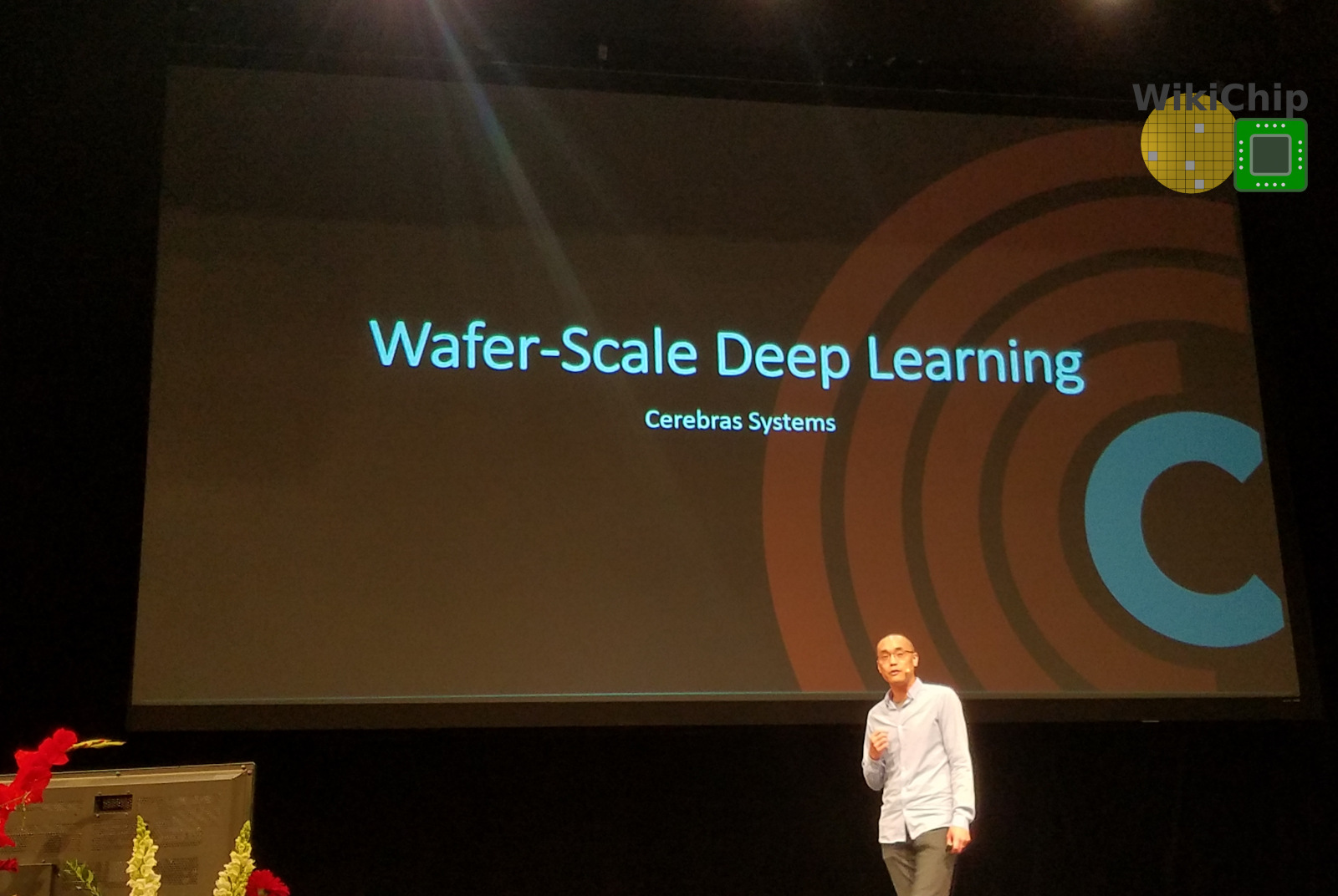
At Hot Chips 31, Cerebras Systems unveiled their new chip – the Wafer Scale Engine (WSE) – and it’s huge. The WSE is a single monolithic one-half square foot piece of silicon!
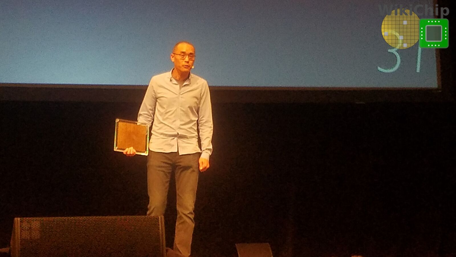
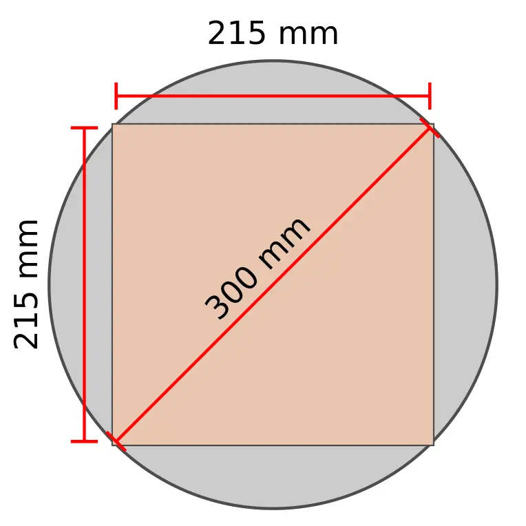
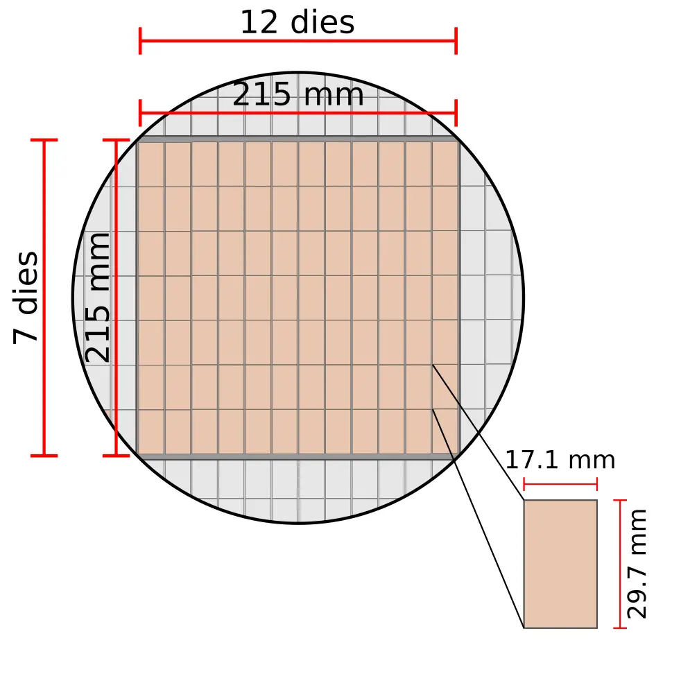
What Cerebras came up with is the largest square chip that can be carved out of a standard 300-millimeter wafer. This is important because Cerebras has partnered up with TSMC and is using its standard 16-nanometer process to manufacture these chips.
The WSE is 215 mm by 215 mm. For those who are rushing to do the math, we’ll save you the effort. 300-millimeter/√2 gives you 212.1 mm. The excess 2.9 millimeters that are outside of the wafer result in the chip having rounded corners.
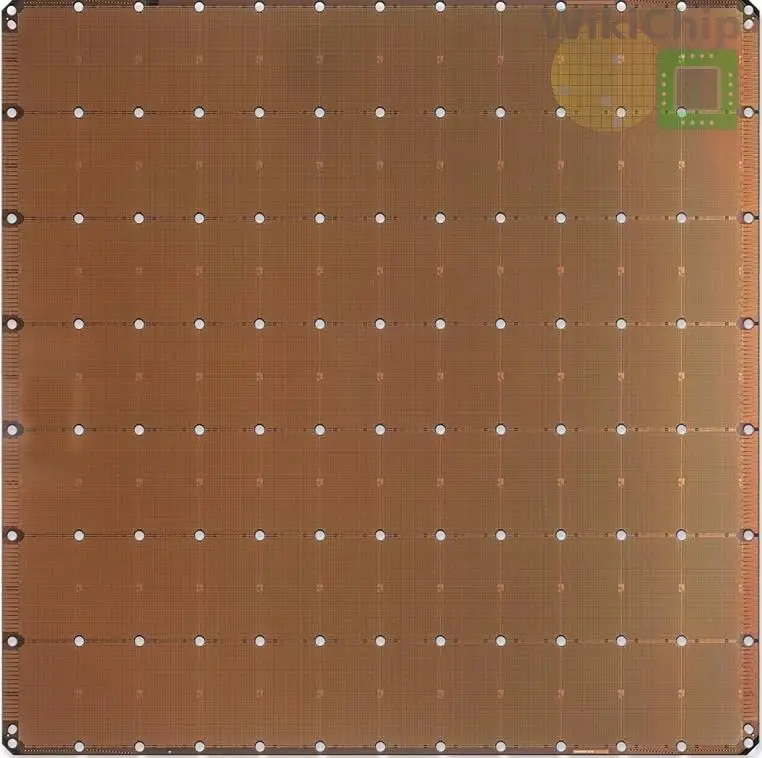
The chip comprises 84 identical dies arranged in a grid of seven by twelve. Each die is roughly 510 mm² with slightly over 4,774 integrated tiny AI core. Cerebras says that there is 1-1.5% of additional AI cores for redundancy reasons which we will touch on in a bit more detail later on. With 84 dies, you are looking at over 400,000 AI cores per chips.
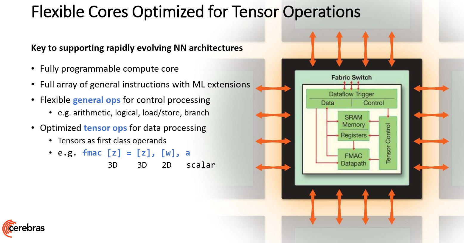
There is a lot that goes on here so we’ll try to summarize the important points. The first part is the cores – almost half a million of them on a single chip. The cores are fully designed by Cerebras for AI workloads. The cores are fully independent and are fully programmable – they are designed to execute their own instruction stream independently of whatever goes on around them. Since the field is evolving, the core design is said to be flexible enough to accommodate new functions and new operations that might be desired in the future. For that reason, the ISA designed by Cerebras comprises both general-purposes operations such as load/store, branch, and arithmetic, as well as a set of tensor operations. The general-purpose operations are your standard CPU operations. Beyond those, Cerebras added native tensor operations that operate on tensor operands. Tensors are first-class citizens on the WSE. In other words, the tensor opcodes accept 2D and 3D tensors directly just like you’d specify registers on a traditional CPU.
As a power reduction mechanism, the cores also support in-hardware sparse processing. The cores do dataflow scheduling with all the compute individually triggered by the data. Cores stall while they wait on useful data which allows them to eliminate unnecessary processing by filter out sparse zero data. It’s also a performance feature to some degree whenever they are able skip past that data and move on to any further available work.
Big Has Its Advantages
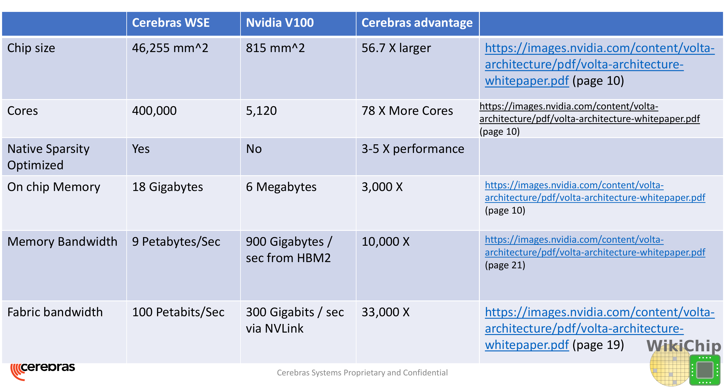
Since there is the equivalent of 84 dies, the numbers are just mind-boggling. This is exactly what Cerebras is promising – a massive performance uplift simply due to the amount of integration. Looking at the comparison between Nvidia’s largest GPU and Cerebras WSE, the numbers are very impressive.
Cerebras Is Selling Boxes – A Full Solution
Due to the complexity involved, Cerebras is not only designing the chip, but they also must design the full system. This allows them to tune it to the right tolerances. Cerebras isn’t disclosing too much about the full product just yet but they have told WikiChip that we can expect more announcements as we get closer to Supercomputing 2019. The WSE will come in 15U units with a chassis for the WSE and another one for the power and miscellaneous components. The final product is intended to act like any other network-attached accelerator over a 100 GbE.
The WSE is close to 57 times larger than the largest GPU in the world – the Nvidia V100. This is impressive, but we need to take a step back and look at what Cerebras is actually offering: one big accelerator. You are not pinning a single WSE against a single V100. The WSE is competing with full Nvidia boxes such as the DGX-2. Without actual benchmarks, it’s hard to tell how the WSE fairs against the DGX-2, but the comparison is much more realistic.
| Cerebras WSE vs Nvidia DGX | |
|---|---|
| Cerebras WSE Box | Nvidia DGX-2 |
| ? | $399,000 |
| ~17.5 Kw* | 10 Kw |
| 84 dies (x57 V100 Si area) | 16 x V100 |
| 16 nm | 12 nm (~ same as 16 nm) |
| No off-chip transfer | 12 NVSwitches |
| 18 GiB SRAM | 96 MiB SRAM (L2) |
| No off-chip memory | 512 GiB |
| >400,000 AI cores | 81,920 CUDA Cores, 10,240 Tensor Cores |
* – Our estimate, calculated at around 15% overhead on top of the WSE
–
Spotted an error? Help us fix it! Simply select the problematic text and press Ctrl+Enter to notify us.
–