
IEDM 2017: Intel details 22FFL, a relaxed 14nm process for foundry customers, targets mobile and RF apps
![]() In March of this year Intel announced their 22FFL process. At the 63rd IEEE International Electron Devices Meeting (IEDM), Intel presented their highly anticipated paper on this process technology. The paper was presented by Dr. Ben Sell, integration manager at Intel.
In March of this year Intel announced their 22FFL process. At the 63rd IEEE International Electron Devices Meeting (IEDM), Intel presented their highly anticipated paper on this process technology. The paper was presented by Dr. Ben Sell, integration manager at Intel.
Overview
While Intel’s regular process technology is geared toward high-performance chips, there is a growing need for a different process that is optimized around a different set of features such as ultra-low power, RF performance, and low design and wafer cost. With those optimizations in mind, Intel developed a new technology called “22 nm FinFET Low Power” or “22FFL” for short. Despite its name, 22FFL borrows more from Intel’s 14nm than it does from their 22nm process. In other words, 22FFL can be thought of as a relaxed 14nm process optimized for mobile and RF applications. “We started with our 14-nanometer transistors and improved from there,” Ben said.
Features
The primary features of Intel’s 22FFL are:
- Low-cost – overall low wafer cost as well as ease of use which lowers designs cost
- High-performance – 14nm transistors were the starting point, adopted for this process
- Ultra-low leakage – special transistors with much lower total leakage than what Intel normally uses for their own technologies
- Low Vmin – Support for low Vmin was needed for reducing the active power
For analog, RF, and I/O functionality 22FFL also features:
- Low noise analog
- High voltage
- High frequency RF
Simplified Metal Stack
For their own products, Intel uses a highly advanced metal stack that offers very tight interconnects that are both complex and expensive to design. 22FFL offers a very simple metal stack with relaxed metal pitches meaning a single-pattern backend flow that reduces cost and is highly flexible and easy to use.
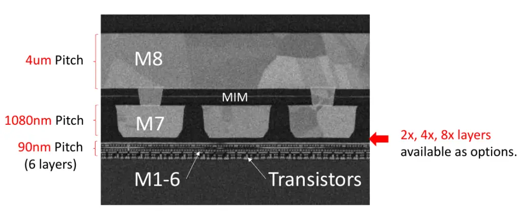
The image above shows the standard 22FFL metallization stack. At the bottom are the transistors on top of which are 6 metal layers with a 90 nm pitch. On top this Intel added two thick metal layers – one with a 1,080 nm pitch and one with a 4-micron pitch. For some applications, adding intermediate layers between the M6 and M7 is very beneficial which is why they offer 2x, 4x, and 8x layers as options.
The two upper layers are designed for global routing. Note that upper-most layer (M8) has a second function – it was specifically designed to be very good for building high-Q inductors (discussed later in this article). Between the M8 and M7, there are the metal-insulator-metal (MIM) capacitors that are used for decoupling the signal capacitance.
Overall, the backend metallization stack is shown below.
| 22FFL Backend Metallization | ||
|---|---|---|
| Layer | Pitch | Note |
| M1 | 90 nm | 1x |
| M2 | 90 nm | 1x |
| M3 | 90 nm | 1x |
| M4 | 90 nm | 1x |
| M5 | 90 nm | 1x |
| M6 | 90 nm | 1x |
| M 2x | 180 nm | 2x option |
| M 4x | 360 nm | 4x option |
| M 8x | 720 nm | 8x option |
| M7 12x | 1080 nm | 12x |
| M8 | 4000 nm | Thick Metal |
High-Performance Logic (FinFET)
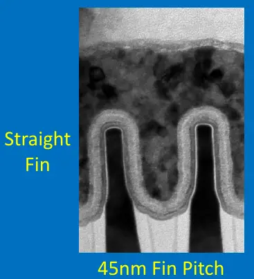
For the high-performance transistors Intel started with their 14nm process FinFET transistors and modified them to suit this new process. Below is a cross sectional view of the fin. What’s immediately clear is that those are Intel’s 14nm very straight fins (their 22nm had trapezoidal fins). The 22FFL fin pitch is slightly relaxed at 45nm (vs 42nm for the 14nm process).
Below is the gate cross section. 22FFL still uses a high-κ metal gate with a strained channel process.
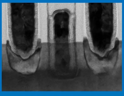
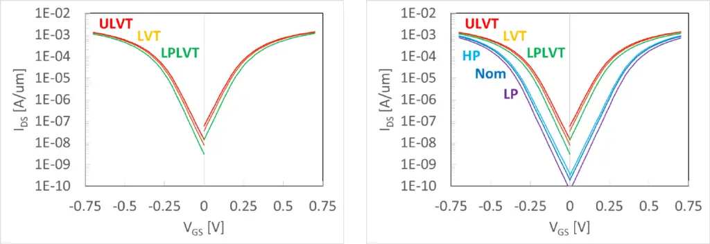
The gate pitch has been greatly relaxed in order to run multiple channel lengths. In case you’re wondering, those dimensions are Lg = 32nm for ULVT and HP, Lg = 36nm for LVT and Nom, and Lg = 44nm for LPLVT and LP. Below on the left are the IDS-VGS curves for those logic devices for both nMOS and pMOS. The figure shows well-behaved devices with a very good DIBL and subthreshold slope. In fact, since the channel effects are so good, they do not get much leakage modulation from the channel lengths so a second work function is used to target the threshold voltage of the remaining devices. This is shown on the second graph on the right.
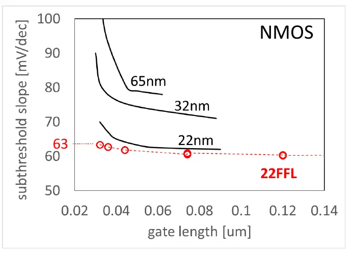
Shown below is the comparison of 22FFL to previous process technologies. FinFET was first introduced by Intel at their 22 nm node which resulted in a much closer to ideal subthreshold slope however once you get down to a very short channel you start to see a sharp increase. With 22FFL, even at the shortest gate lengths (i.e., 32 nanometers), Intel still reports 63 mV/dec subthreshold slope meaning very close to linear. With 22FFL intel offers analog devices and those feature a much larger gate length of up to 160 nm. Those analog devices stay at around 60 mV/dec.
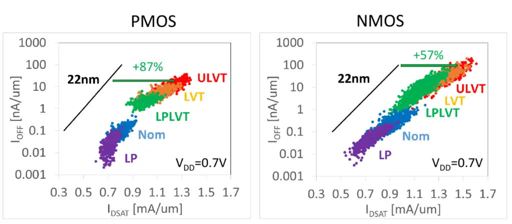
At 0.7 volt, Intel reports 1.29 mA/μm for pMOS and 1.38mA/μm for nMOS for their highest performance devices. Compared to their own standard 22 nm technology, there is a significant improvement in drive current for both pMOS and nMOS. For pMOS Intel reported 87% increase in drive strength and 57% increase for nMOS. Note that for the low-leakage devices (shown in purple and blue on the graph below), 22FFL has considerably higher drive current and lower leakage vs. what they had for their standard 22nm process.
–
Spotted an error? Help us fix it! Simply select the problematic text and press Ctrl+Enter to notify us.
–