
Intel launches Gemini Lake
Intel has finally launched their latest low-power processors for value embedded, mobile, and desktop computers. Code-named Gemini Lake, those SoCs feature an improved core, their latest graphics architecture, and a new set of wireless features.
Codename Decoder
Before we delve into the new product offering, we need to make sense of Intel’s codename zoo. Below is a simple codename decoder.
| Codename Decoder | ||
|---|---|---|
| Last Generation | This Generation | |
| Microarchitecture | Goldmont | Goldmont Plus |
| Processor Core | Apollo Lake | Gemini Lake |
| Families | Pentium Celeron |
Pentium Silver Celeron |
Pentium Silver
With this launch Intel has also introduced Pentium Silver. Previously Intel included SKUs based on their low-power architectures along with the mainstream high-performance architectures under the same Pentium brand name. Now low-power SKUs will go under the Pentium Silver family with the high-power SKUs under the Pentium Gold. The new naming scheme should hopefully making it easier to distinguish the two types of processors.
![]()
Changes
The new products, codename Gemini Lake, are based on the new Goldmont Plus microarchitecture. Keeping up with Intel’s new tradition, the specific improvements done have not been detailed. We do know that the new graphics are based on Gen9.5 like Kaby Lake and Coffee Lake but they have pulled in Gen10-related display features. The cache has also doubled to 2 MiB per core duplex for a total of 4 MiB. We’ve also managed to confirm that Gemini Lake is fabricated on Intel’s “14nm” process (not their enhanced flavors 14nm+ or 14nm++).
The new cores should have support for a number of new instructions:
- SGX – Software Guard extensions
- UMIP – User-mode instruction prevention
- PTWRITE – Trace logger write user data
- RDPID – Read Processor ID
New CNVi integration
The new Gemini Lake models integrate a new “Connectivity Integration” (CNVi) block. The CNVi moved most of the expensive functionality of a connectivity chip on-die including the MAC components of the Wi-Fi and Bluetooth cores, the processors, logic, and memory. The only thing not included is just the signal processing, analog and RF functionality which will stay in the “Companion RF” (CRF) module for the time being (although those will likely move to the processor as well in due time). This extra integration will help greatly with the BOM of low-cost mobile devices.
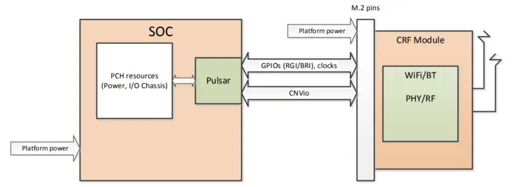
It’s worth noting that the same integration is expect for mobile Cannon Lake processors, albeit this will be integrated onto the chipset instead of the processor itself.
New SKUs
| Processors | |||||
|---|---|---|---|---|---|
| Model | Cores | L2 | Clock | GPU | GPU Clock |
| Desktop SKUs (10 W TDP) | |||||
| J4005 | 2 | 4 MiB | 2,000 / 2,700 MHz | UHD Graphics 600 | 250 / 700 MHz |
| J4105 | 4 | 1,500 / 2,500 MHz | UHD Graphics 600 | 250 / 750 MHz | |
| J5005 | 4 | 1,500 / 2,800 MHz | UHD Graphics 605 | 250 / 800 MHz | |
| Mobile SKUs (6 W TDP / 4.8 W SDP) | |||||
| N4000 | 2 | 4 MiB | 1,100 / 2,600 MHz | UHD Graphics 600 | 200 / 650 MHz |
| N4100 | 4 | 1,100 / 2,400 MHz | UHD Graphics 600 | 200 / 700 MHz | |
| N5000 | 4 | 1,100 / 2,700 MHz | UHD Graphics 605 | 200 / 750 MHz | |
Note that regardless of the core count, all SKUs have 4 MiB of L2 cache implying that for the dual-core parts, only one core from each duplex is active. Additionally, all SKUs support up to 8 GiB of dual-channel DDR4/LPDDR4 up to 2400 MT/s.
–
Spotted an error? Help us fix it! Simply select the problematic text and press Ctrl+Enter to notify us.
–