
Hot Chips 30: AMD Raven Ridge
AMD series of APUs based on the Zen microarchitecture were first introduced in late 2017. Earlier this year, AMD further extended their selection to desktop market. Those are complete system-on-chip solutions that incorporate both the central processor and the graphics processor on the same chip. At Hot Chips 30, the chip design was presented by Dan Bouvier, Client Products Chief Architect at AMD.
Raven Ridge
Ryzen with integrated Vega graphics, formerly codename Raven Ridge, are AMD’s latest full SoC solutions for both desktops and mobile. The chip incorporates a quad-core Zen CPU Complex along with an AMD Vega GPU with 11 CUs.
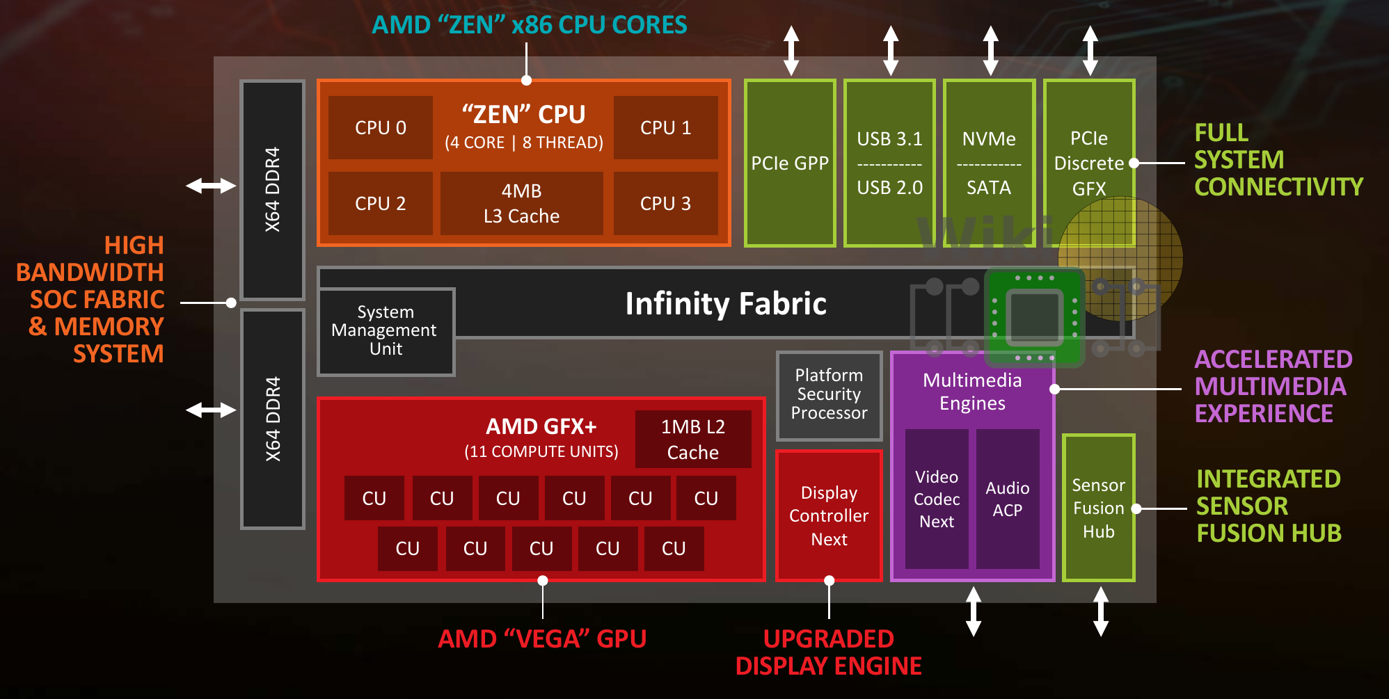
Bouvier explained that Raven Ridge was a clean sheet design. This provided them with a unique opportunity to rework many of the components on the chip. A brand new display engine was incorporated along with a new video codec engine, and new audio processor. There is also a new I/O subsystem sporting USB 3.1 along with native USB-C connectivity.
Die
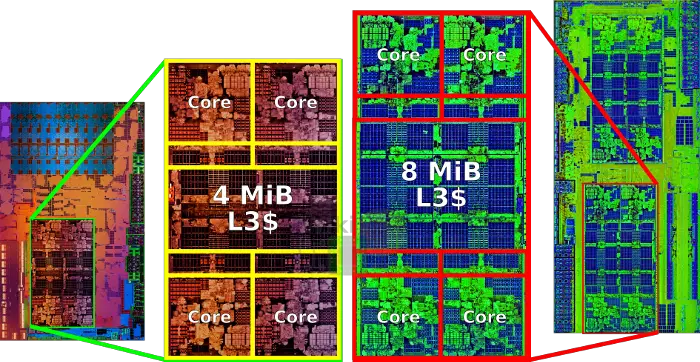
The chip itself is a single monolithic die measuring 209.78mm² packing 4.94 billion transistors and is fabricated on GlobalFoundries 14nm process. This works out to a 0.84x shrink over Bristol Ridge which was made on GlobalFoundries 28nm (28SHP) after adding 1.84B more transistors.

For Raven Ridge, AMD uses a quad-core Zen CCX with a slightly reduced cache. That is, instead of the full configuration with 8 MiB of L3, Raven Ridge has half of that, at 4 MiB.
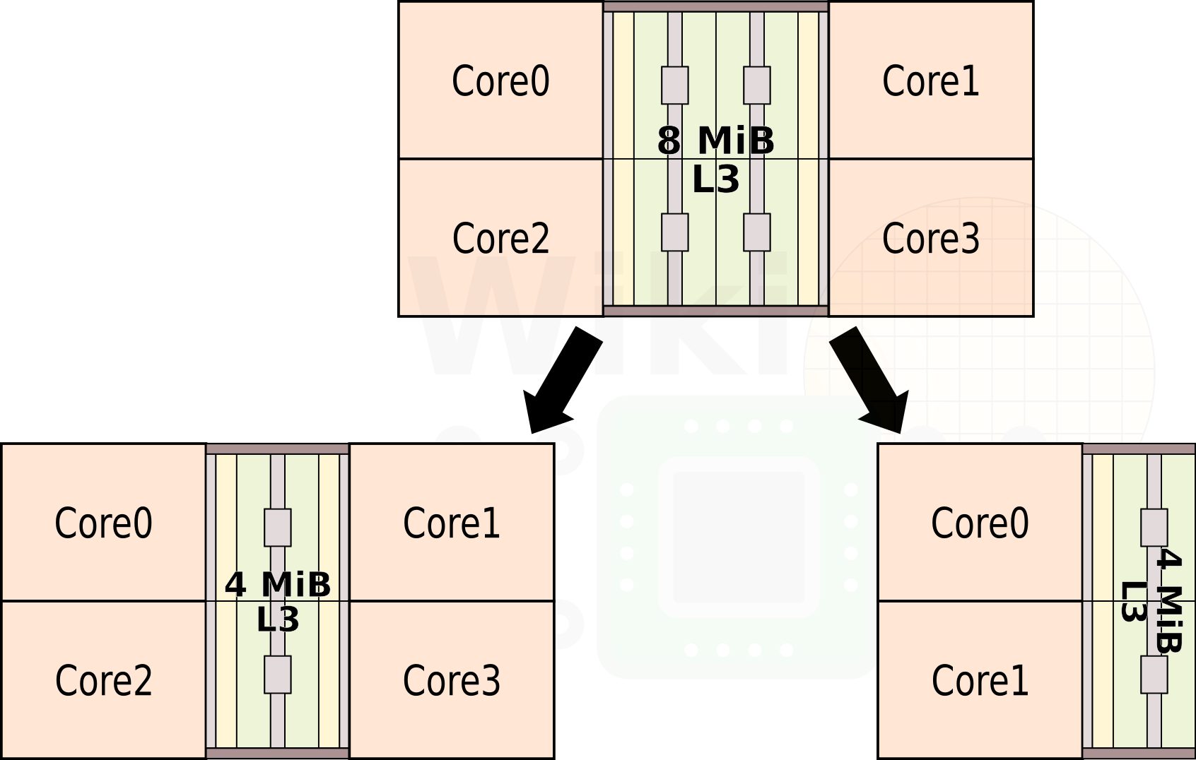
It’s worth pointing out that Bristol Ridge did not have a level 3 cache. The new cache helped not only in improving the core performance, but by significantly reducing the system-level traffic. This was very important as it improved the effective bandwidth going to the Vega GPU.
Vega
For this design, AMD increased the amount of silicon area dedicated to the GPU. The GPU is the same design as the Vega cards but slightly reduced in resources. There are 11 compute units and 1 MiB of a large dedicate level 2 cache for computing and texture caching.

With 11 compute units, there are 704 shaders, 44 TMUs, and 16 ROPs. Bouvier stated that the max frequency targeted was 1,200 MHz. This would put the maximum theoretical performance at 845 FLOPS (DP), 1690 FLOPS (SD), and 3,379 FLOPS (HP). By the way, AMD already released some parts with slightly higher frequency, thus slightly higher peak compute.
–
Spotted an error? Help us fix it! Simply select the problematic text and press Ctrl+Enter to notify us.
–