
ISSCC 2018: Intel’s Skylake-SP Mesh and Floorplan
![]() Earlier last month, the 65th International Solid-State Circuits Conference (ISSCC) was held in San Francisco. This year Intel presented their Skylake server system architecture. The paper was presented by Dr. Simon Tam, senior principal engineer at Intel’s Scalable Performance CPU Development Group.
Earlier last month, the 65th International Solid-State Circuits Conference (ISSCC) was held in San Francisco. This year Intel presented their Skylake server system architecture. The paper was presented by Dr. Simon Tam, senior principal engineer at Intel’s Scalable Performance CPU Development Group.
Skylake-SP
Intel’s Skylake server architecture marks a significant departure from previous generations. Substantial modifications took place to the core itself, beyond the microarchitectural changes that Skylake brought along with the client processors. Those changes were done in order to better address the datacenter market segment. The four major modifications are:
- Support for the AVX-512 extension with 32 double-precision floating point operation per cycle per core
- Data center-workload optimized cache with a 1 MiB L2 per core and 38.5 MiB of non-inclusive distributed but shared L3
- A new mesh architecture with low-latency interconnect
- Hexa-channel DDR4, Ultra-path Interconnect (UPI), PCIe Gen3, and Omni-Path Fabric
For an exhaustive list of changes, check out our Skylake server microarchitecture article.
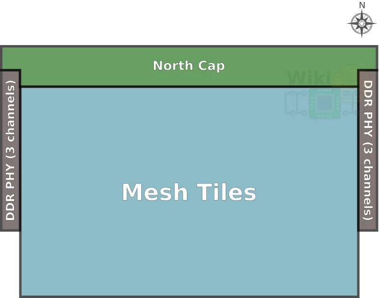
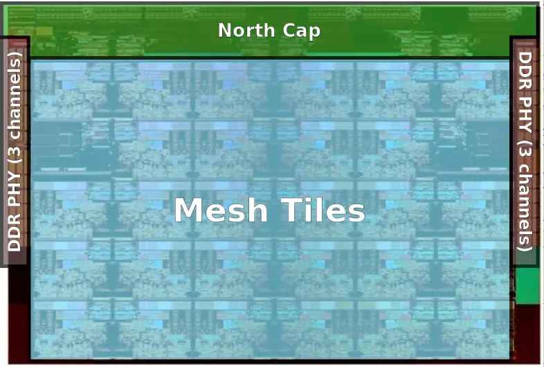
Floor-Plan
The 28-core Skylake microprocessor die is a superset of everything the Skylake has to offer. The smaller core count variants are a strict subset which can be inferred from the large die. Regardless of the die variant, there are three major areas:
- DDR PHYs
- North Cap
- Mesh Tiles
DDR PHYs
There are two independent and identical physical sections of 3 DDR4 channels each which reside on the east and west edges of the die. Each channel is 72-bit (64 bit and an 8-bit ECC), supporting 2-DIMM per channel with a data rate of up to 2666 MT/s for a bandwidth of 21.33 GB/s and an aggregated bandwidth of 128 GB/s. RDIMM and LRDIMM are supported.
Data bytes are located on the north and south sub-sections of the channel layout. Command, Control, Clock signals, and process, supply voltage, and temperature (PVT) compensation circuitry are located in the middle section of the channels. Presumably, the layout is something like this.
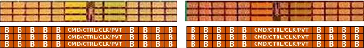
It’s worth pointing out that the location of the PHYs was carefully chosen in order to ease the package design. Specifically, they were chosen in order to maintain escape routing and pin-out order matching between the CPU and the DIMM slots to shorten package and PCB routing length in order to improve signal integrity.
North Cap
The top of the die is called the North Cap and it contains all of the I/O PHYs, I/O agents, serial IP ports, and the fuse unit.
At the very top of the North Cap are the various I/O connectivity. There are a total of 128 high-speed I/O lanes – 48 PCIe lanes (3×16) operating at 8 GT/s, x4 DMI lanes for hooking up the Lewisburg chipset, 16 on-package PCIe lanes (operating at 2.5/5/8 GT/s), and 60 (3×20) Ultra-Path Interconnect (UPI) lanes operating at 10.4 GT/s for the multiprocessing support.
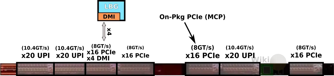
At the south-west corner of the North Cap is the clock generator unit (CGU) and the Global Power Management Unit (Global PMU).

The North Cap interfaces with mesh (discussed later on) via the CMS which are located at the bottom of the North Cap itself.
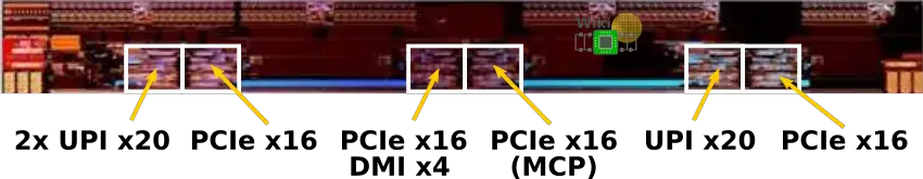
It’s interesting to note that the first two UPI links share the same interface with the mesh. This is in contrast to all other I/O links which have their own dedicated mesh station stops.
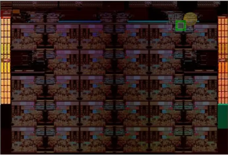
Mesh Tiles
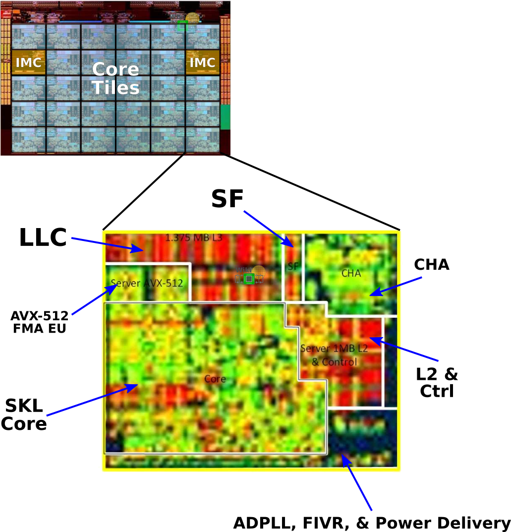
The third major component of the die is the mesh which consists of a 2-dimensional array of tiles. There are two types of tiles: core tiles and IMC tiles. We have annotated the tiles on the Skylake die below.
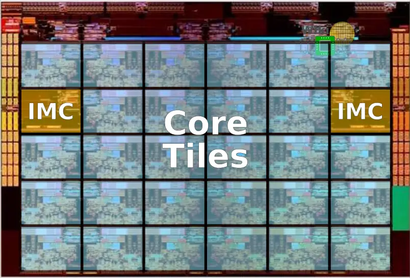
The majority of the tiles are core tiles. Those consist of the Skylake core, the caching and home agent (CHA), the snoop filter (SF), and the last level cache (LLC) which in this case is also always the L3. Each core also features an all-digital PLL, fully-integrated voltage regular (FIVR), and the accompanying power delivery subsystem. Intel has provided a 400x zoomed in picture of the core. Although it is rather blurry, it’s still relatively easy to see the large macro blocks.
Last year when Intel launched Xeons processors based on this Skylake, they explained that the client core was extended with the added functionality. Interestingly, if we take the Skylake client core it’s not too hard to see how Intel derived the server core by augmenting it with the specific server architecture functional blocks.
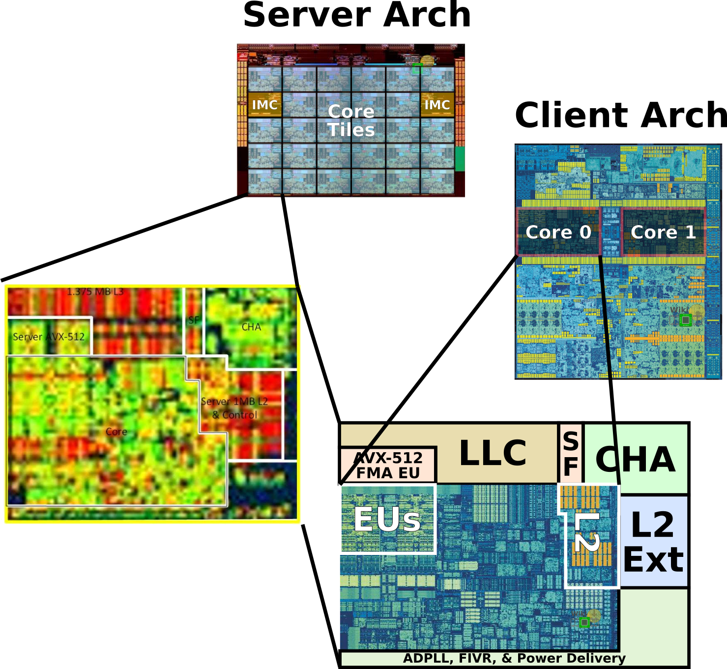
At the north-east corner of each core is the second AVX-512 execution unit. It’s extending the client core execution units which are located just below. Each one of those units is capable of executing up to 32 double-precision floating point operations per cycle. The standard client Skylake core has a 256 KiB L2 cache organized as 1024 sets by 4 ways. The new server L2 is now a much larger 1 MiB organized as 1024 sets by 16 ways. Intel claims the new larger cache is much more optimized for the virtualization workloads that is done in the data center. It’s worth pointing out that the larger cache has added two additional latency cycles.
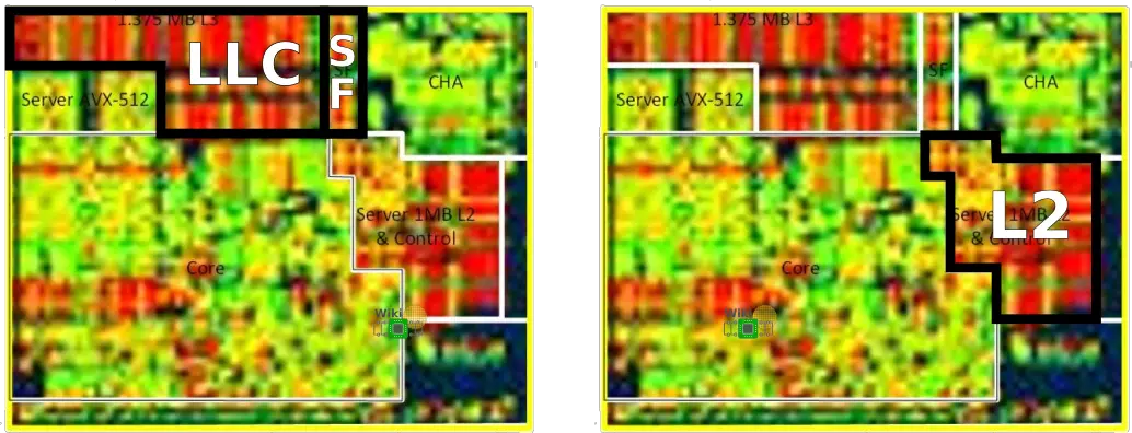
At the top of the core tile is the last level cache (LLC) and the snoop filter (SF). The L3 is 1.375 MiB and is non-inclusive of the lower caches. The L3 is organized as 2,048 sets by 11 ways while the SF is 2,048 sets by 12 ways. In previous architectures, Intel had a shared LLC that was inclusive. The SF is now tasked with the bookkeeping job of tracking resident L1/L2 cache lines that have been evicted from the L3.
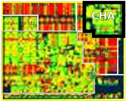
At the very north-east corner of each tile is the caching and home agent (CHA) block. The CHA, as its name implies, acts as the cache agent for the core. The CHA also interfaces with the 2D fabric via the CMS. The way this is done is discussed later.
Modularity and Scalability Goals
A key design goal of the Skylake server floor plan was to be modular as well as scalable. The purpose of the tile is to enable this modularity and scalability by incorporating all the necessary building blocks inside the tile itself. Once done, the tile can then be duplicated over across multiple rows and columns. This design allows Intel to tile in both the X and Y directions.
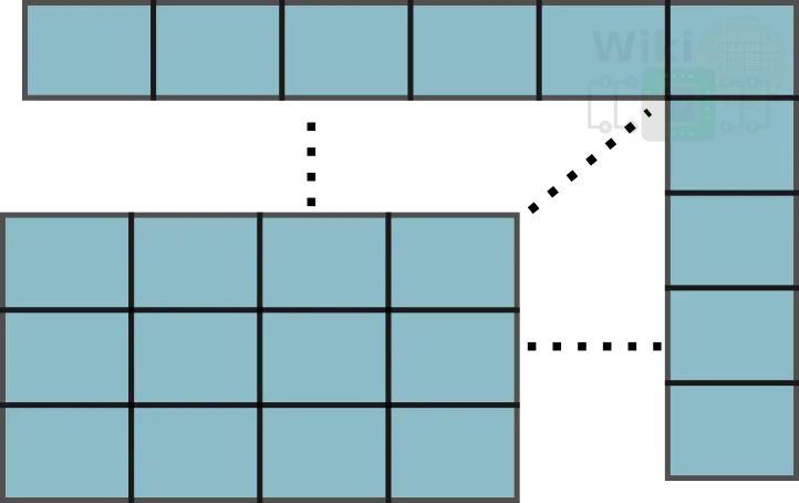
Note that Intel is already using this modularity in order to create multiple processor derivatives. Their low core count (LCC) die features a 3 by 4 grid of 12 tiles and 10 cores while their high core count (HCC) contains a 5 by 4 grid of 20 tiles with 18 cores. It would be interesting to see how this floor plan evolves as Intel moves to their 10 nm process.
–
Spotted an error? Help us fix it! Simply select the problematic text and press Ctrl+Enter to notify us.
–