
ISSCC 2018: Intel’s Skylake-SP Mesh and Floorplan
Mesh
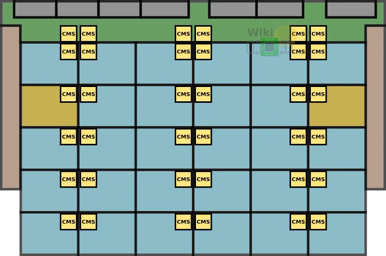
The Skylake server dies contain a new mesh fabric which succeeds the previous ring bus interconnect. The architecture itself is almost identical to what had been implemented in the Xeon Phis based on the Knights Landing microarchitecture. The mesh is synchronous, high-bandwidth, and can scale to a much larger number of core tiles. Compared to the previous ring design, the 2D mesh provides considerably higher the bi-sectional bandwidth. At least as far as the large die (the 28-core one) goes, there are 36 converged mesh stops (CMS). The CMS is the common stop between four points on the mesh and serves as the mechanism to switch between half rings on the mesh. In other words, the CMS is the interface between all the various subsystems and the mesh interconnect. We have highlighted the locations of the CMSes on the die below.
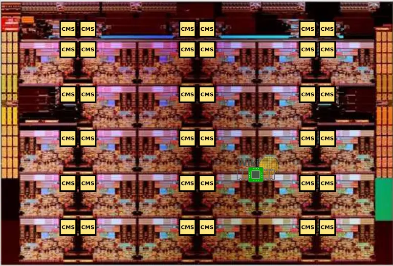
It can be seen that the location of the mesh stops is in the same physical location as the CHA of each tile. It’s worth noting that most of the mesh is likely routed above the cores in a similar fashion to how Intel has done it with the ring interconnect which was wired above the caches in order reduce the die area.
Each core tile interfaces with the mesh via its associated converged mesh stop (CMS). The mesh stops at the very top are for the UPI links and PCIe links to interface with the mesh (those were annotated on the previous page). Additionally, the two integrated memory controllers have their own CMS they use to interface with the mesh as well.
Every stop at each tile is directly connected to its immediate four neighbors – north, south, east, and west.
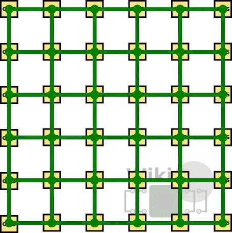
Every vertical column of CMSs form a bi-directional half ring. Similarly, every horizontal row forms a bi-directional half ring.
By the way, although Intel uses the term “bus” sometimes to describe their rings and half rings architectures, as with the mesh half ring, those are very much point to point interconnects.
Routing
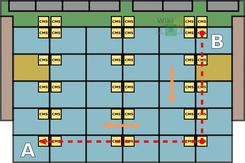
A great benefit of having a mesh is that packet can now take the shortest path to reach their destination. The routing algorithm is extremely simple and is identical in operation to the Knights Landing implementation – packets are first routed over the vertical half ring and then over the horizontal half ring. Switching between a vertical and horizontal half ring means the packet is taken off the first ring and is placed on the second ring.
For example, to get from point A located at the very south-west corner of the die to point B located at the very north-east corner, the packet is first routed all the way north to the appropriate row and is then routed eastward to the correct tile.
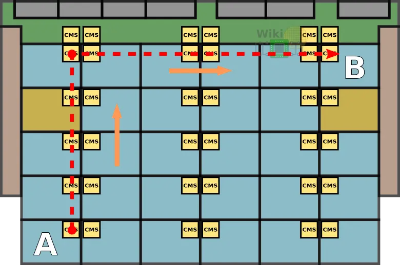
Note that the response from B to A will be taking a different route – first vertically to the very south-east tile and then horizontally, to the destination at the south-west tile.
Performance Implications
Because all packets follow the same vertical-first-horizontal-second algorithm, the performance characteristics of the mesh is dictated by the Y axis routing latency. With the help of some power domain optimizations (will be discussed in a future article), Intel has achieved single-cycle vertical title-to-tile latency at frequencies above 2 GHz without affecting the power of the rest of the uncore. It goes without saying that for complex consumer-producer applications, understanding the behavior of the mesh and the physical locations of the cores is important in order to choose superior core pairs.
A need for Scalability, Modularity
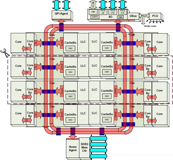
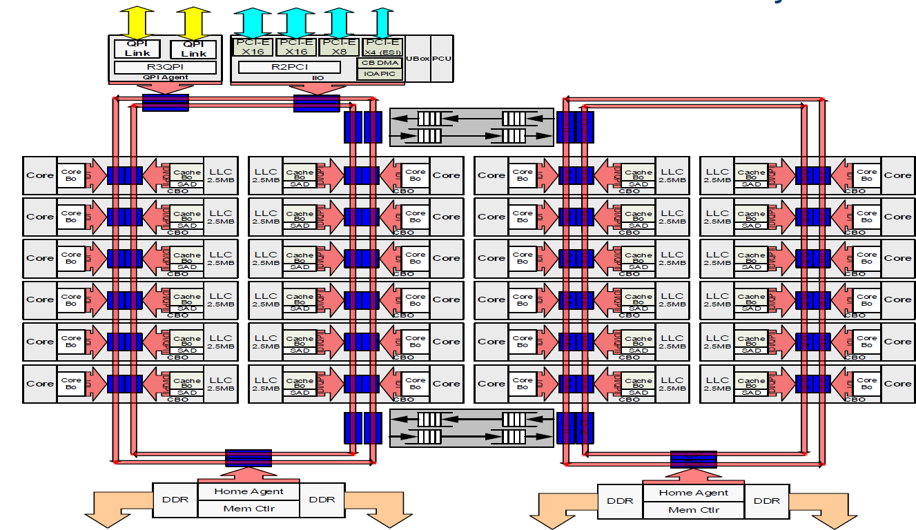
Over the past decade, Intel has been refining their ring interconnect architecture to suit an ever-growing core count. Unfortunately, with each generation, the added cores increased the access latency while introduction addition traffic and lowering the effective per core bandwidth. They mitigated this problem by splitting up the die into two halves, each on its own ring. This reduced hopping distance and added additional bandwidth but it did not solve the growing fundamental problems of the ring.
 |
 |
| Sandy Bridge vs Broadwell | |
Among the many goals of the Skylake server architecture was a new high-bandwidth scalable and modular architecture that could scale well for years to come. The final product successfully addressed those design goals. The mesh interconnect replaced the prior ring, allowing their high-end models to reach as much as 28 cores on a 30-tile mesh. A modular tile architecture was developed, enabling Intel to reuse the IPs to target a wide range of markets. This is achieved by the addition and removal of rows and columns of tiles to easily create floor-plan derivatives for different die configurations for different markets.
Derived WikiChip Articles: Mesh Interconnect, Skylake (Server)
–
Spotted an error? Help us fix it! Simply select the problematic text and press Ctrl+Enter to notify us.
–