
Intel Expands 22FFL With Production-Ready RRAM and MRAM on FinFET

Embedded flash is hitting a scaling wall around the 16/22 nanometer nodes. Additionally, as SRAM scaling becomes ever more challenging, companies look to other technologies for a possible alternative and complementary solutions. Intel has been continuously improving its 22-nanometer 22FFL process. Both RRAM and MRAM are two of the leading candidates for replacing embedded flash. Earlier this year, at the VLSI Symposium, the company announced that both RRAM and MRAM are production-ready on their 22FFL platform with bit yield rate of greater than – a low-power high-performance process primarily designed for cost-sensitive analog, wireless, edge, automotive, and IoT applications. Both technologies have been demonstrated with a bit yield rate of greater than 99.9%.
For more info on Intel’s 22FFL see: IEDM 2017: Intel details 22FFL, a relaxed 14nm process for foundry customers, targets mobile and RF apps
1T-1R
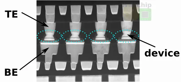
Both RRAM and the STT-MRAM use the same 22FFL design rules and very similar infrastructure. In fact, both devices use the very same layout, likely to simplify design and manufacturing. Both bitcells are 1 transistor – 1 resistor (1T-1R) design embedded between the Metal 2 and Metal 4 layers.
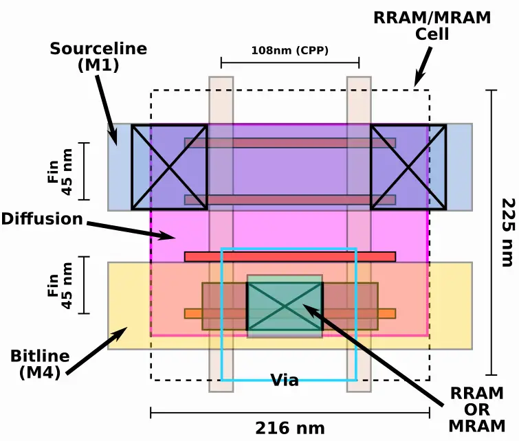
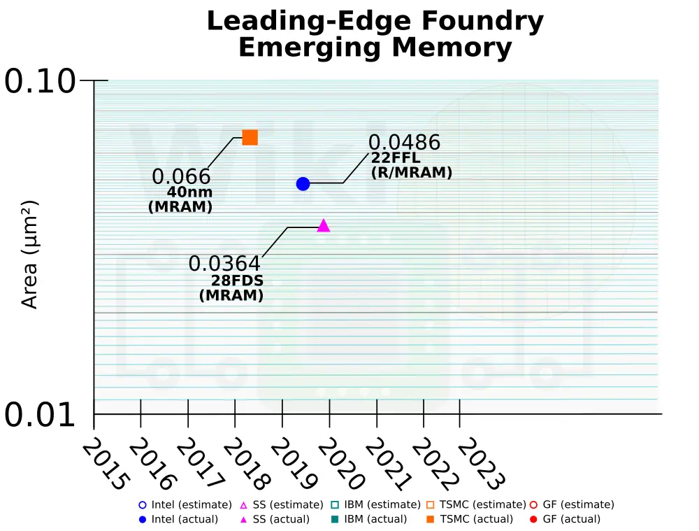
Each cell is 216 nm by 225 nm for a total area of 0.0486 µm². Additionally, there is a high retention RRAM cell which measures 288 by 225. The high-density cells use 2 poly word lines, a bit line on Metal 4, and a source line on Metal 1.
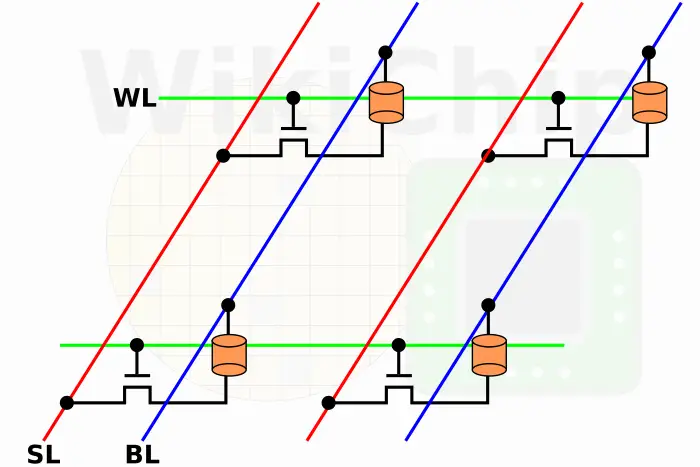
Though their write mechanism and operation is very different, the high-level behavior for both are very similar – they act as a variable resistor with the resistance sensed in order to determine the stored value. A basic array will look something like this.
22FFL RRAM
The CDs for RRAM here is 100-150 nm. The cell themselves use the 22FFL high-voltage transistors consisting of four fins. As noted earlier, there are RRAM cells offered. The 216 nm by 225 nm is the high-density cell. Additionally, there is a high retention cell which measures 288 by 225. They have slightly AEC-Q100 grades. The high density cell is capable of Grade 3 automotive temperature range (-40 degrees to 85 °C degrees). The high retention cell supports Grade 2 automotive temperature range (-40 to 105 °C).
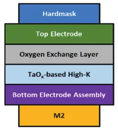
Intel uses a Tantalum Oxide-based (TaOx) stack. On top of the Metal 2 layer, you have the bottom electrode (BE), tantalum oxide, High-K, Ta-based oxygen exchange layer (OEL), and the top electrode. Finally, a metallic hard mask is used on top. Following anneal, oxygen is redistributed, leaving you with a layer of vacancies at the interface between the OEL and the Tantalum Oxide layers.
Applying a high enough voltage (somewhere around 1.5 V) with the right polarity, the bit storage is formed. Applying voltage in the opposite polarity will reset the bit, leaving it in the high-resistance state (HRS). Applying voltage in the same polarity that was used for forming will set the bit, leaving it in a low-resistance state (LRS).
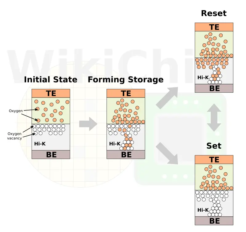
Typical LRS resistances are in the 3kΩ to 7kΩ while the typical HRS is in the 20kΩ to 40kΩ. Intel demonstrated read sense time of 5 ns at 0.7 volts (or 10 ns at 0.5 V) with a write time of 10 μs. Read energy is less than 1 pJ/bit.
A problem with RRAM is that cycling through fundamentally modifies the filament by shifting of oxygen ions, thus altering the cell characteristics. Cycling between LRS and HRS slowly causes oxygen ions to get lost to the OEL. By the way, the act of driving oxygen out of the switching medium is irreversible. Loss of ions over time means more current must be pumped each time to reset the device. The crossover point in which the current available from the transistor is no longer sufficient to hit HRS is the point at which the cell is no longer operable.
For Intel’s RRAM, after 10,000 switching cycles, not much degradation in the LRS state is observed. However, the HRS starts requiring a significant increase in current after 10,000 cycle in current to achieve the desired resistance which is the limiting factor for their 10K switching cycle endurance. Retention experiences the opposite effect – requiring maintenance of the LRS state. To that end, Intel reported a bit error rate of less than 10e-7 for uncycled bits and 1e-5 for arrays after 20K switching cycles.
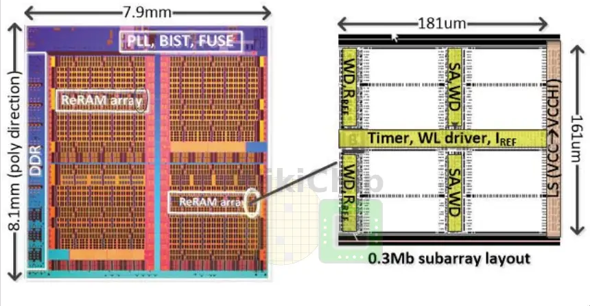
Earlier this year, at the IEEE ISSCC 2019, Intel demonstrated a high-density RRAM macro. The details of the macro itself are beyond the scope of this article but we will discuss its performance and density characteristics later on. Intel is able to achieve 10.1 Mb/mm².
22FFL STT-MRAM
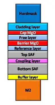
The target device CDs here is between 60 nm and 80 nm. STT-MRAM cells rely on a Magnetic Tunnel Junction (MTJ) for storage. The junction comprises one tunnel barrier layer sandwiched between two two ferromagnetic layers – a free layer and a reference layer. The free layer can have varying magnetic directions while the reference layer maintains a fixed magnetic direction. The bit is stored as the magnetic orientation in the free layer. When both layers align in the same direction (i.e., when the magnetic field is parallel for both layers), the device is in a low resistance (P) state. Likewise, when the two layers have opposite directions, the device is in a high resistance (AP) state.
Intel’s STT-MRAM uses a dual-MgO MTJs with a CoFeB-based free layer.
Intel demonstrated 4 ns read sensing time at 0.9 V (down to 8 ns at 0.6 V). The bit cell exhibit a write endurance of 10e6 cycles with a read disturb of 1e12. As far as retention goes, Intel reported 10-year retention not only at the Grade 2 automotive temperature range (-40 to 105 °C) but also at 200 degrees C for 10 years which is much higher than anything else we are aware reported to date.
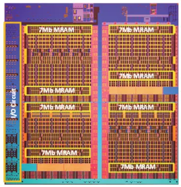
For their MRAM, Intel also demonstrated a high-density MRAM macro. They reported achieving a density of 10.6 Mb/mm².
Comparison
Emerging memory technologies like MRAM and RRAM promises to pick up where embedded flash left off. To that end, Intel is reporting very promising numbers for its 22FFL MRAM and RRAM technologies. There are, however, a number of areas of weaknesses such as low endurance.
| Intel Memory Comparison | |||||
|---|---|---|---|---|---|
| MRAM (22FFL) |
RRAM (22FFL) |
SRAM (22FFL) |
SRAM (14nm) |
SRAM (10nm) |
|
| Type | non-volatile | non-volatile | volatile | volatile | volatile |
| Size (µm²) |
0.0486 | 0.0486 | 0.087 | 0.0499 | 0.0312 |
| Density (Mb/mm²) |
10.6 | 10.1 | 6.551 | 11.6 | 23.6 |
| Read | 4 ns @ 0.9 V 8 ns @0.6V |
<5 ns @ 0.7 V <10ns @ 0.5V |
~ ns | ~ ns | ~ ns |
| Write | <1 µs | <10 µs | ~ ns | ~ ns | ~ ns |
| Endurance | >1e6 | >1e6 (write) >1e12 (read disturb) |
>10e15 | >10e15 | >10e15 |
- 1 – WikiChip estimates
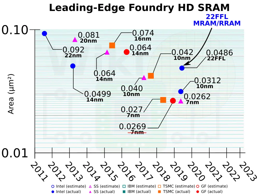
One small peculiarity about Intel’s MRAM and RRAM is that the bitcell sizes are much larger than one might expect given the feature sizes of 22FFL. Despite being close to double the density of the SRAM on the same process, the cells are still close to 2-3x the size you’d expect. For example, Samsung’s own STT-MRAM for its 28 nm (planar) FDSOI process features a considerably denser bitcell size of 0.0364 µm². This could have been done intentionally to simplify design and manufacturing for their first design. Nonetheless, there is room for improvement.
–
Spotted an error? Help us fix it! Simply select the problematic text and press Ctrl+Enter to notify us.
–