
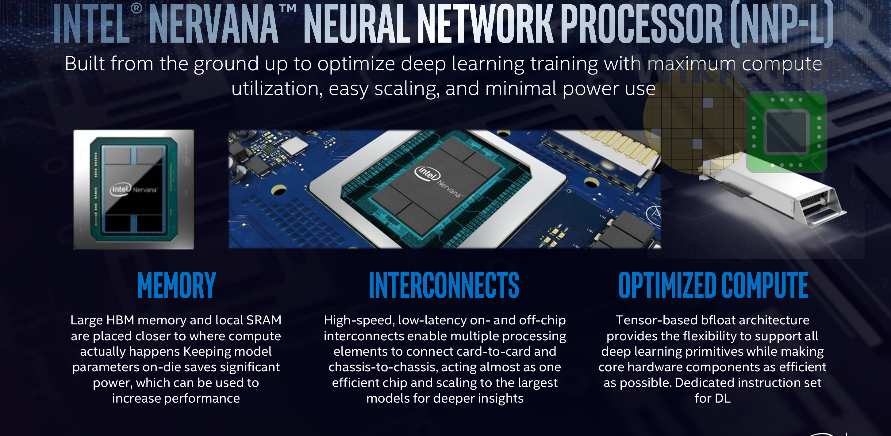
Intel’s Spring Crest NNP-L Initial Details
In 2016 Intel acquired Nervana Systems in the hope of expanding beyond their traditional CPU market with more specialized ASICs. The company’s first-generation Neural Network Processor (NNP) was a 28-nanometer design called Lake Crest. This chip served as a software development vehicle without making it to general availability.
Spring Crest
Intel’s follow-up design is Spring Crest. It was first announced at last year’s Intel AI Developer Conference. Last week at the Linley Spring Conference Carey Kloss, VP of Intel AI Products Group and GM for AI Hardware, gave some of the first initial details of their AI accelerator. Carey Kloss. along with Andrew Yang, lead the original Nervana Systems hardware development effort. Intel’s AI products are branded as the Intel Nervana Neural Network Processors (NNP). The NNP-L product family targets data center machine learning/training while a second family, the NNP-I, will target inference. The first series of products will start with the 1000 series. Kloss main talk was about the NNP L-1000 accelerator. We will lightly touch on the inference chip as well.
The NNP-L is fairly straightforward architecturally compared to the designs of some of the AI startups out there, though Nervana did make interesting design choices. At a high level, the NNP-L accelerator tries to maximize the off-die memory. It includes 32 GiB (x4 stacks) of HBM2, no cache, and very localized SRAM. The NNP-L is only about accelerating deep learning training as much as possible. This largely means doing convolutions and matrix multipliers (though there are some additional functions). To that end, the NNP-L tries to integrate as many multipliers on-die as possible. There is no free lunch and with many multipliers, they must be kept fed. When dealing with ‘nice’ matrices, this works out quite well. Given a large matrix (e.g., 1k x 1k x 1k or even 4k x 4k x 4k), due to the number of columns, you are able to reuse the same data element 1000s of times after reading it just once from memory. This results in a design with very high utilization – at least in theory. In practice, real-world matrices are seldom as nice and often show up in different sizes and especially odd shapes (e.g., tall and skinny, short and fat). Those matrices force hardware to waste a lot of time moving data back and forth, causing lower real-world utilization. Intel tries to balance the two by optimizing for more realistic problems in order to maintain a higher compute utilization and higher data reuse from the HBM.
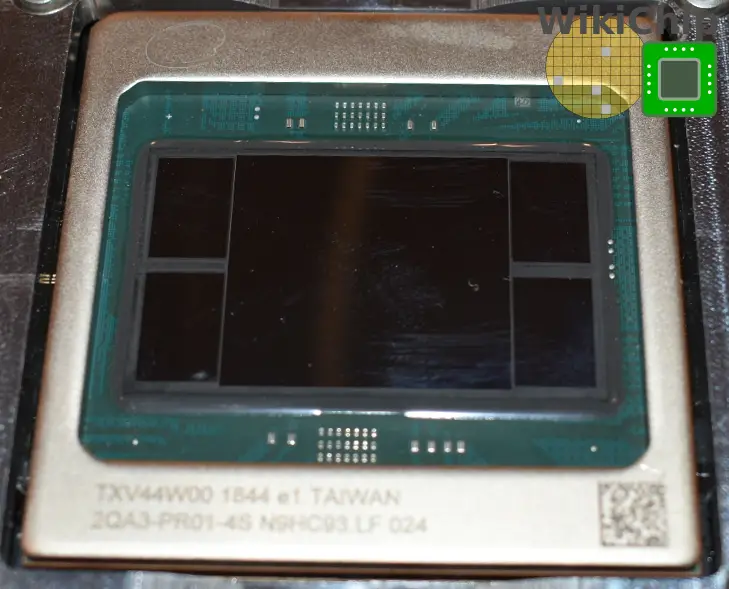
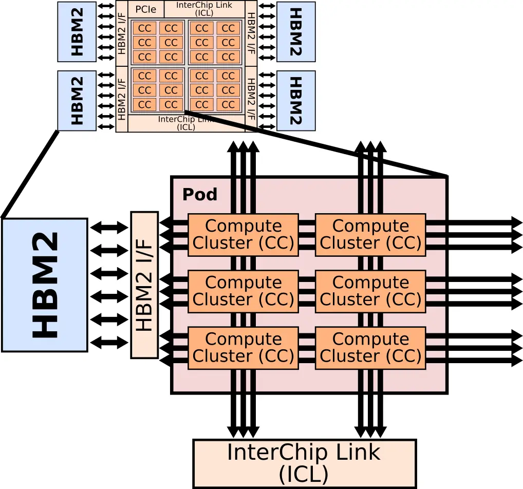
The die itself is impressively large. We estimate it at roughly 26 mm by 28.5 mm (741 mm²), this is likely Intel’s largest die. It’s worth noting that it is manufactured by TSMC on their 16-nanometer process.
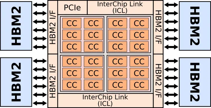
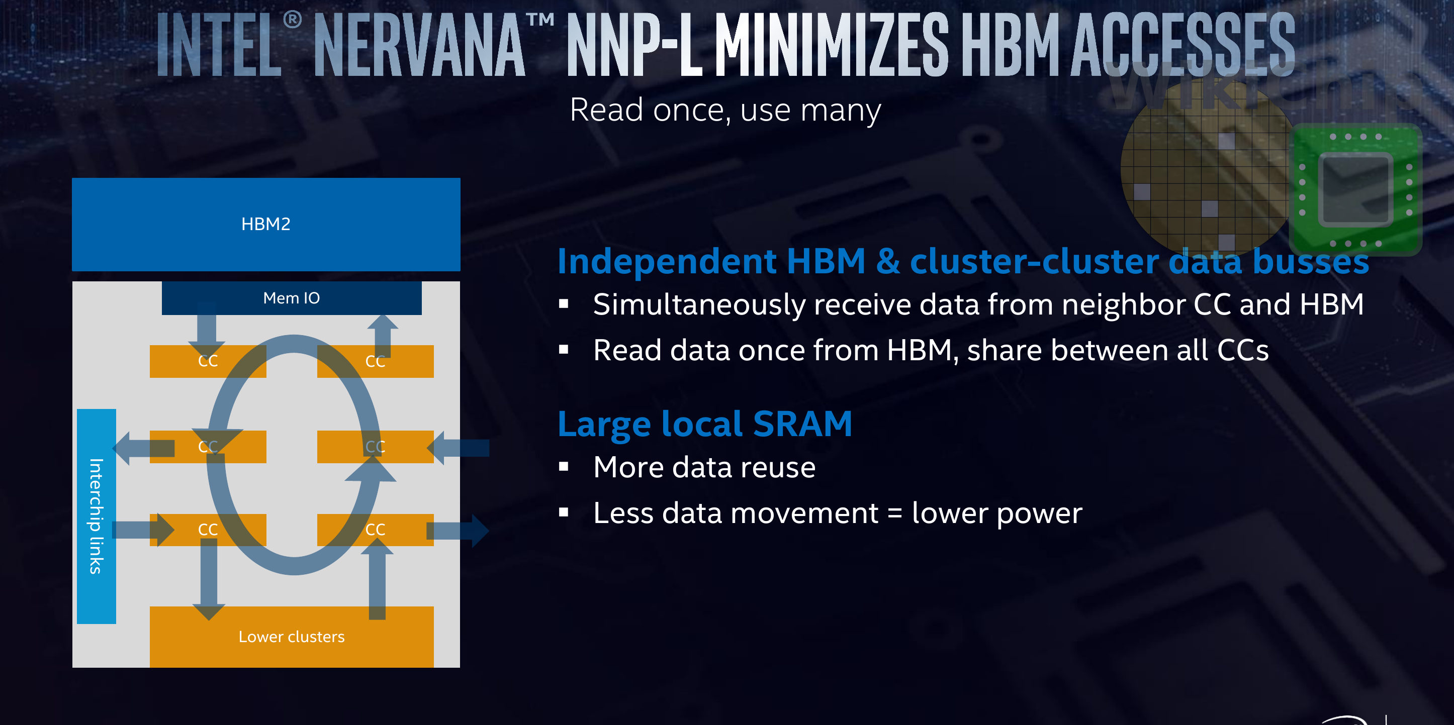
The chip has four pods, one at each of the quadrant. Each pod includes six compute clusters (CCs) and is directly linked to the nearest HBM. Intel stated that every aspect of the architecture was designed to increase the number of times they can use each piece of data that is read from DRAM – all in order to directly increase the compute utilization of the chip.
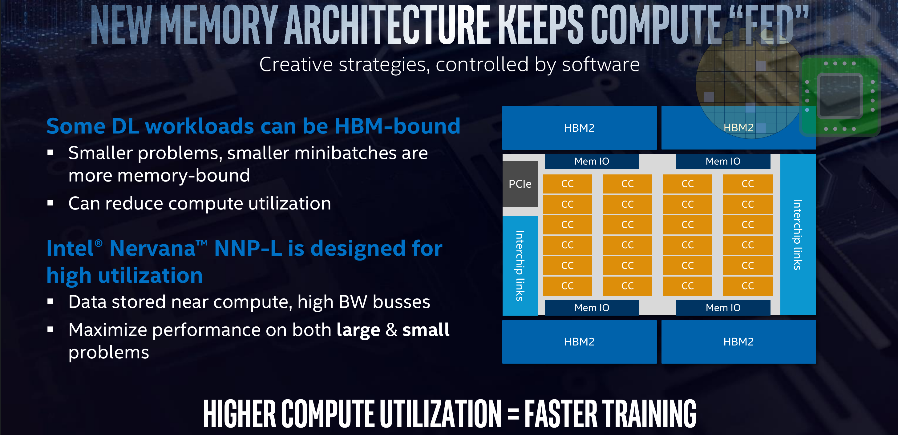
Within each pod are six compute clusters (bigger dies having a higher amount). Instead of opting for 1000s of compute elements, the NNP-L features much larger compute clusters capable of handling matrix multipliers of “reasonable size”. Each of the compute clusters incorporate a large amount of SRAM as well. This is done to help the software. The chip memory is statically allocated with the software controlling what’s in the HBM as well as the compute clusters. The idea here is to predetermine the best place for data in order to maximize reuse by keeping it where it’s going to be used the most. In theory, this should also help with utilization by keeping the computer clusters busy.
Each pod is connected to its own HBM, to the external InterChip interconnects (ICLs), and to neighboring pods. There is a massive amount of bandwidth going in every direction. Within each pod are three full-speed bidirectional buses (actually full meshes) in all four directions from each of the compute clusters. There are multiple connections between those buses and the HBM interface as well as multiple connections to the InterChip Links. In order to exploit parallelism, those buses operate simultaneously and at full speed in order to facilitate many tasks at the same time. For example, some pods may be transferring data to other pods, while some compute clusters may be operating on the previous results of another compute cluster, while another cluster is writing the data back to memory, and another cluster reading memory back on-chip. As noted earlier, software statically schedules everything in an attempt to maximize data reuse and data fetches for higher utilization.
Utilization Performance Claims
Intel disclosed just initial compute utilization numbers comparing Baidu’s DeepBench Nvidia DGX-1 with the V100 utilizations to the NNP-L. Testing was done on the NNP-L A-stepping pre-production silicon operating at 900 MHz (lower than final clocks). The intention here is to show the benefit of the architectural choices they have made. Note that actual training performance numbers will be disclosed later this year.

BFloat16
In their original design, Lake Crest, Nervana used the flexpoint integer-based numeric encoding format they developed. Intel says that based on their study of bfloat as well as through customer feedback, they have pivoted to bfloat16. The brain floating-point format reduces the mantissa bits while keeping all the exponent bits from the standard IEEE float32 data type. This means you keep the dynamic range but sacrifice some precisions. Intel says that based on their own testing and customer feedback, everyone is largely satisfied with this format.
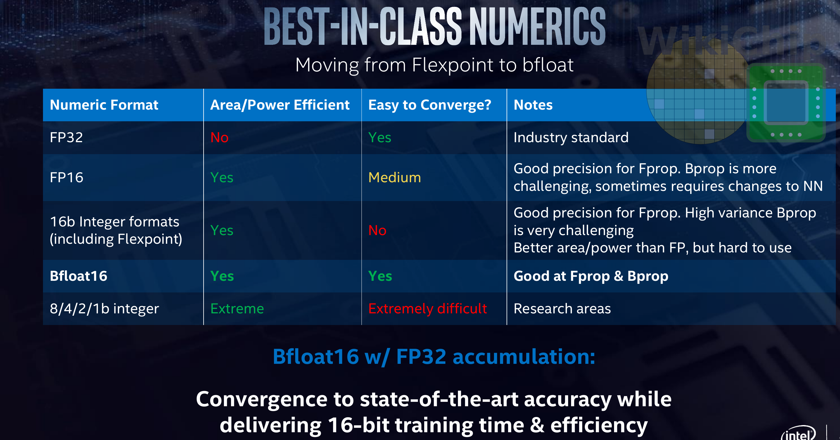
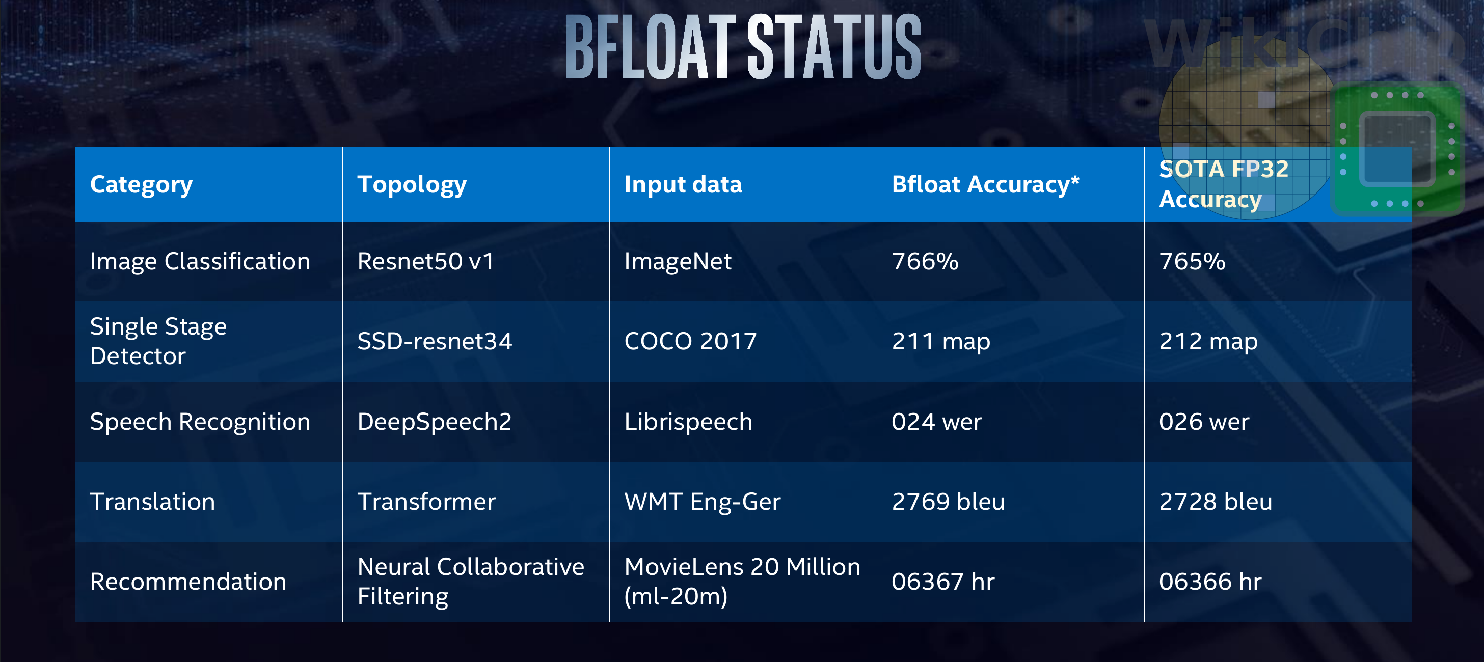
The table below was presented, comparing bfloat to standard float32 (although some functions still remain FP32 e.g. master weights, constants, and accumulation). Note that was done on simulated results prior to actual silicon. Using the same models, Intel is reporting similar accuracies to FP32. Similar results were reported last year by Google which has also implemented bfloat16.
Packaging
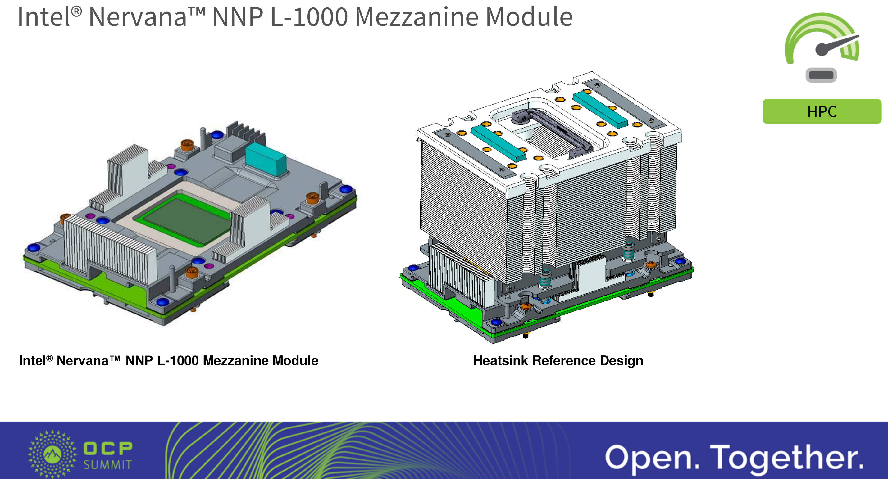
The NNP-L will be available in PCIe form but more interestingly it will also be available as a mezzanine board based on the OCP Accelerator Module (OAM) design specification. This is expected to be the first product to make use of the OAM design and is one of the first accelerators to gluelessly extend beyond a single node from chassis to chassis (note that current Nvidia solutions are only possible through complex use of switches). The OAM design was unveiled earlier last month at the OCP Summit by Song Hang. The OAM is quite a complex design, involving high-density PCB routing, component placement, connector selection, and baseboard and chassis design. The module is 102 mm by 165 mm with specs supporting 48 V and up to 700 W (or 300 W for 12 V). Intel’s module design is somewhat simplified by using 48 V with power consumptions limited to 200 W and 425 W.

The final board design which gets shipped to customers is down below. A heatsink reference design is also provided in order to speedup development but customers may also opt for other cooling designs.
Scalability
The NNP-L supports both data and model parallelism distributions. In data parallelism, operations are split up with each chip having the whole model and its own data and the final weights are shared and gathered together. This is relatively easy. In model parallelism, the same data is used by all the chips but for a different portion of the model. Due to the high communication complex, generally, this is much harder to do. Intel is targeting the ability scale to very large models with model parallelism. They believe that companies will continue to grow their models to gain better insights and it will not be possible to use a single chip but instead will require a large number of chips to handle those models. To that end, the NNP-L packs as many high-speed interconnect links as they could put on the die’s perimeter. With the large number of SerDes, depending on the number of mini-batches, Intel expects near-linear scaling.

Note that although the graph above shows scaling to up to 64 chips, Intel says that from a system point of view, there is no limitation as to how high it can scale.
A lot of effort has gone into ensuring easy glueless scaling between dies. For large problems that do not fit in the local HBM or for problems that can exploit the parallelism across multiple dies and get a near-linear speedup, it’s advantageous to take advantage of the NNP-L scalability. It’s worth noting that given the order of magnitude difference in bandwidth between the on-die interconnects and the off-die SerDes, problems need to be sufficiently large in terms of compute to justify all the data movement.
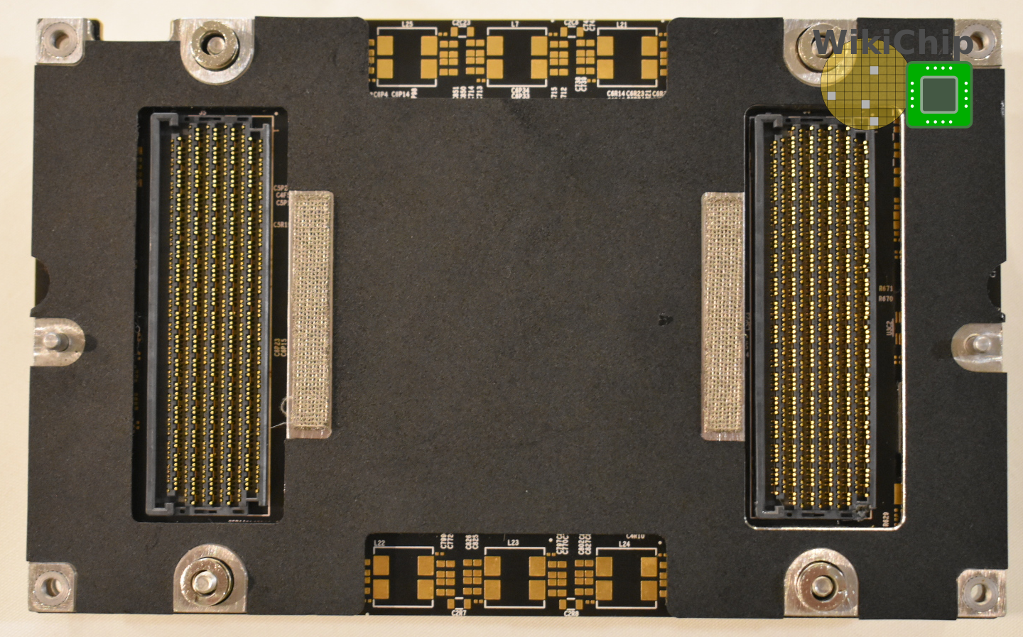
The InterChip Links (ICP)s are not one of Intel’s existing technology but were custom designed low latency, low overhead, reliable transmission links. The NNP OAM module comes with 16 ICL SerDes ports, with each port being x4 lanes. The OAM module defines up to 7 x16 SerDes ports in order to support multiple interconnect topologies. In the NNP case, the 16 x4 SerDes are combined into 4 x16 (4×4) SerDes. In the OAM module, this corresponds with SerDes 1, 3, 4, and 6 in the specs.

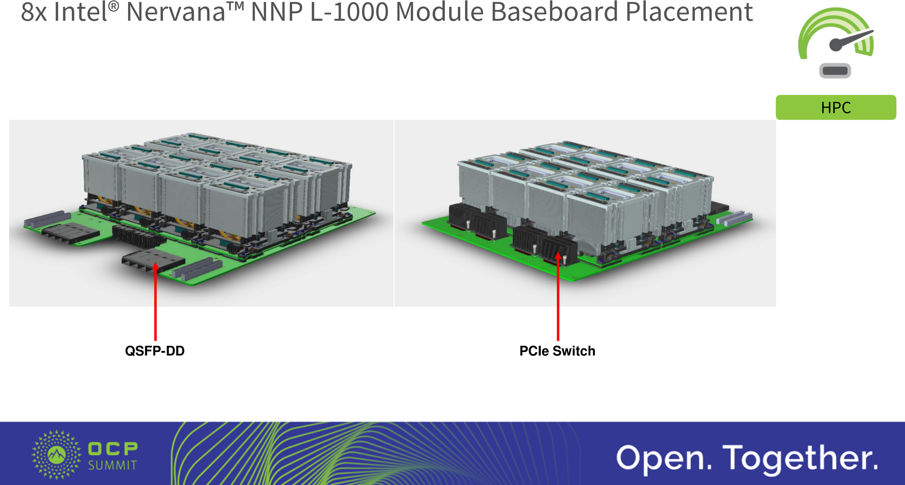
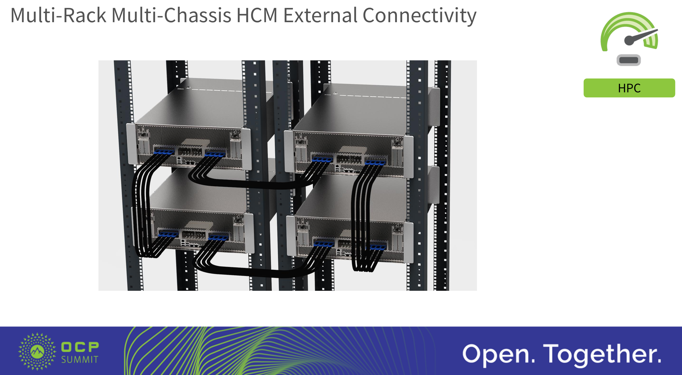
Intel is providing customers with a baseboard reference design which incorporates up to eight NNP L-1000 modules. The NNP module supports 40-60 V with a total of 3400 W (8 x 425 W NNP-Ls). The board design is fairly simple, featuring a PCIe switch on the one side with the NNP modules in the middle and the QSFP-DD for chassis-to-chassis interconnects.
When a single node is used, the QSFP-DD cables are simply linked back to the same chassis.
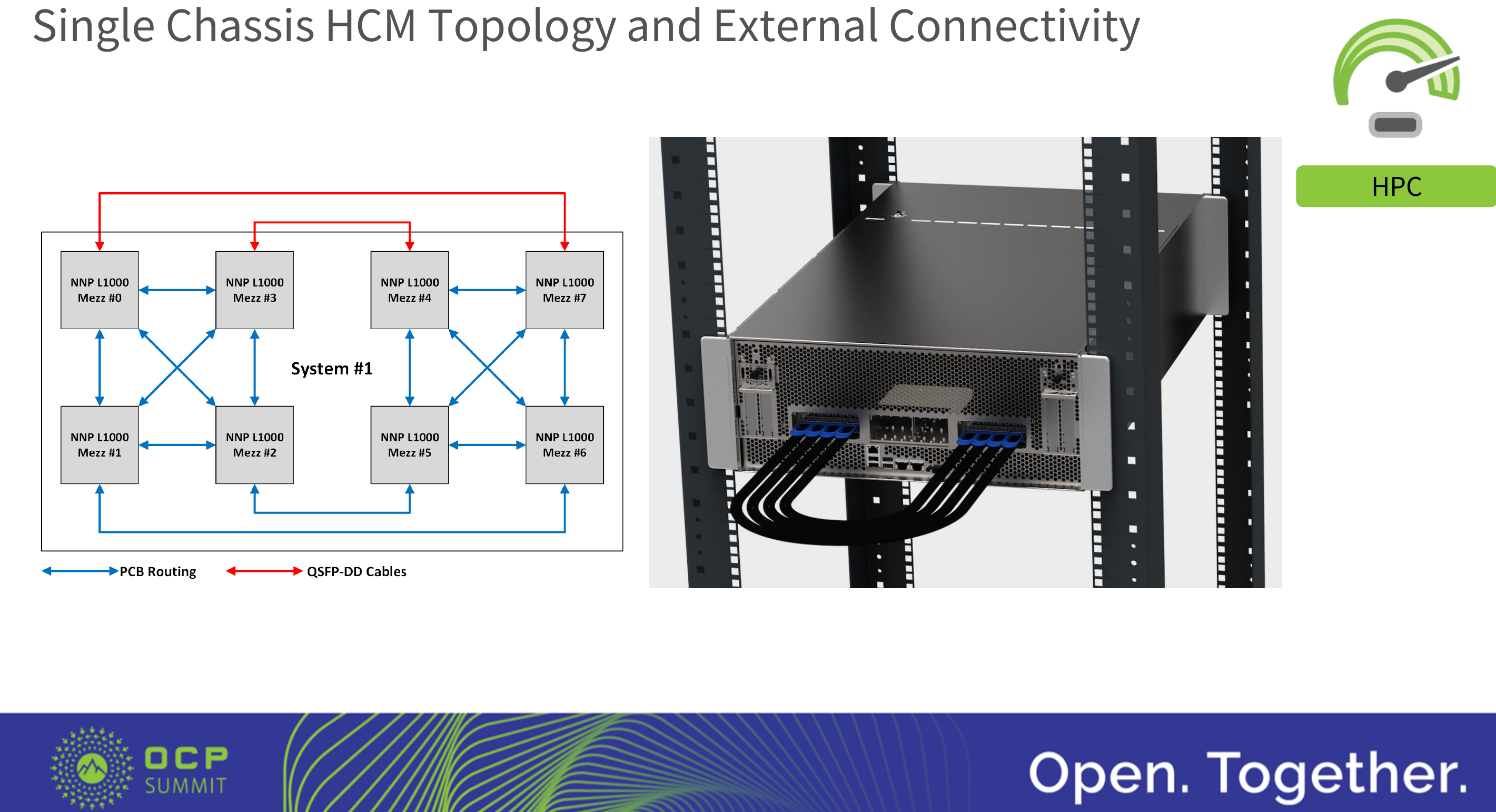
When extending the hybrid cube mesh to two nodes, the four QSFP-DD ports now link between the two nodes.

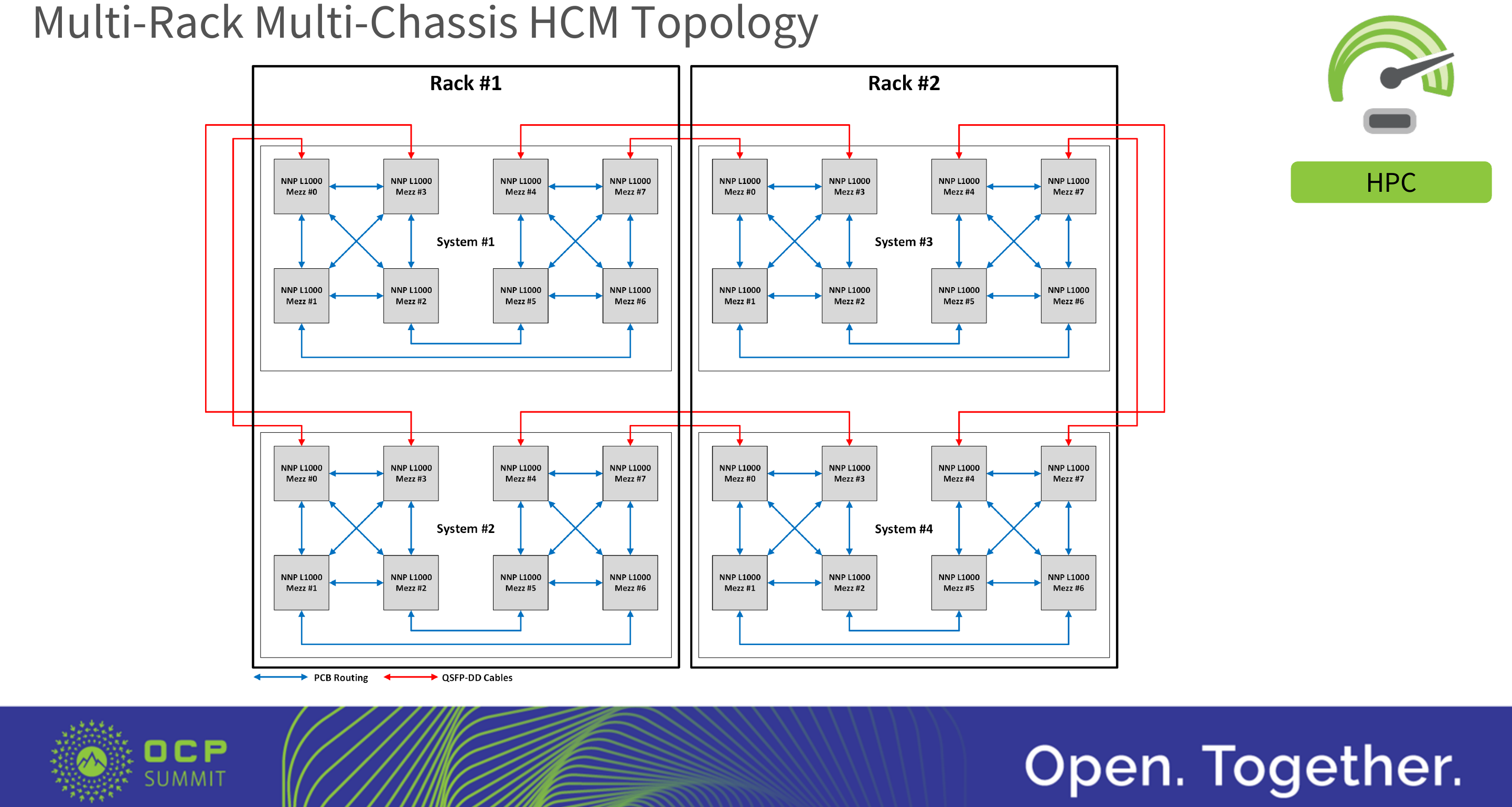
Intel also proposed a multi-rack multi-chassis hybrid cube mesh topology for customers that asked for much larger configurations.
Inference
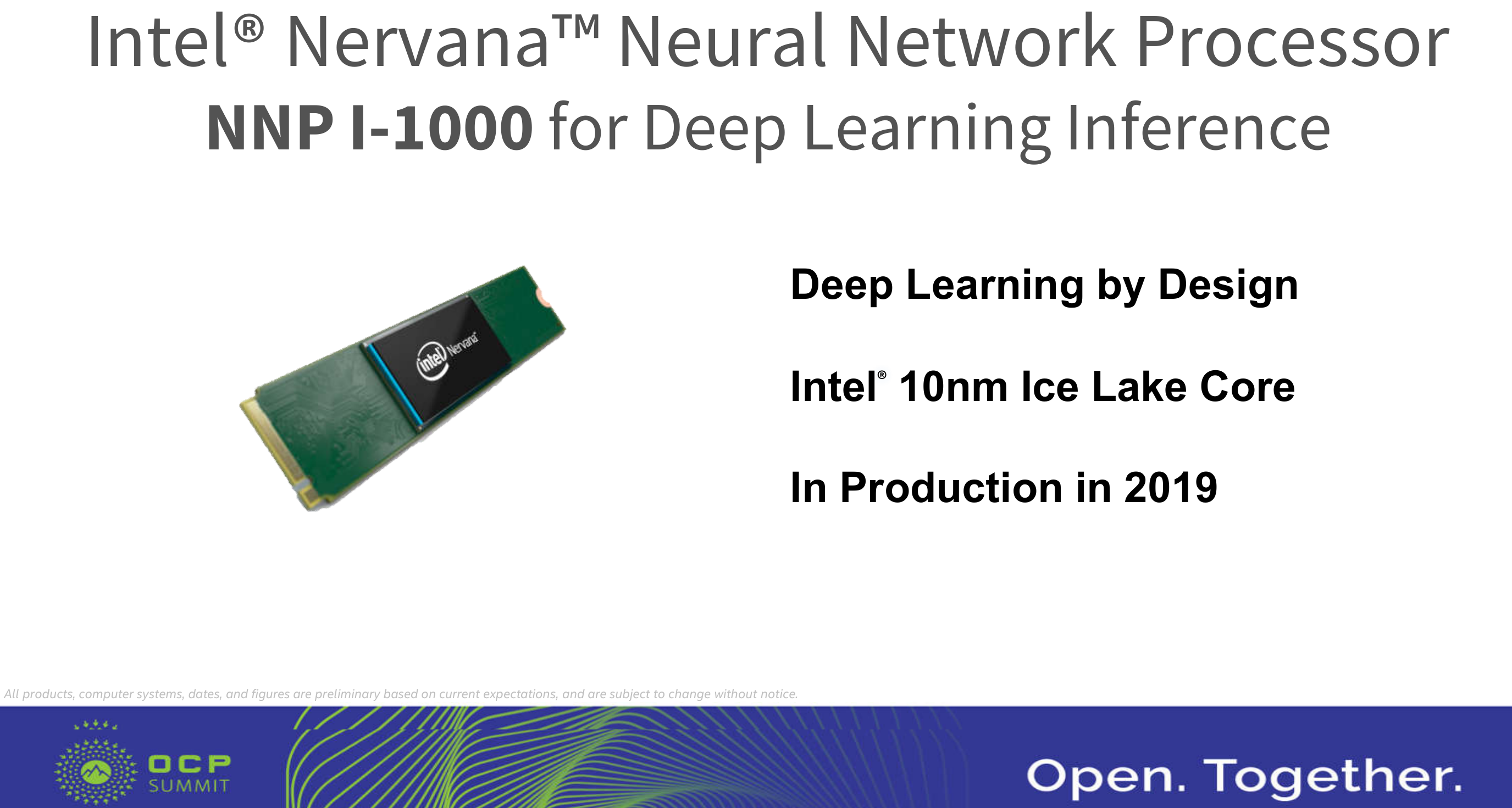
Intel considers their Xeons to be the backbone for inference. We have recently seen the launch of Cascade Lake which brought DL Boost (AVX-512 VNNI) designed specifically for the acceleration of inference workloads. Those workloads tend to be tightly integrated with other workloads such as server and transactional workloads which is why they are a great fit for CPUs. Intel has also announced the NNP-I, presumably codename Spring Hill. This is a dedicated inference accelerator product. It is an M.2 device, manufactured on Intel’s 10-nanometer process, and will leverage Sunny Cove.
Production
With the NNP-L A-stepping in testing, B-stepping is expected to come back in the coming months. Intel says that both the NNP-L and NNP-I will be launching later this year.

Derived WikiChip articles: Intel Nervana NNP
–
Spotted an error? Help us fix it! Simply select the problematic text and press Ctrl+Enter to notify us.
–