
TSMC Demonstrates A 7nm Arm-Based Chiplet Design for HPC
 As chiplet-based designs shift gear from research to production, we see a new influx of chiplet papers from industry. Earlier this month, at the 2019 VLSI Symposium which was held in Kyoto, Japan, TSMC demonstrated their own chiplet design.
Challenge and Demo
Using a chiplet-based design has a few notable advantages such as faster development cycle and improved yield and thus cost, but it comes with a new set of challenges. Those challenges stem from the pursuit of a monolithic-like power and performance characteristics in a chiplet-based design. Consequently, two of the chief challenges are the interconnects and packaging technology. Although those challenges remain open questions, multiple solutions with varying properties were proposed. At the VLSI Symposium, TSMC demonstrated a number of their own technologies that attempt to address those challenges.
The three main properties TSMC was attempting to validate were:
- Arm cores operating at > 4 GHz
- BiDir Interconnect Mesh Bus at > 4 GHz
- CoWoS and LIPINCON at 8 GT/s and < 1 pJ/bit
It’s important to note that this research and technologies validation was intended for high-performance computing. For that reason, it features cores with very high clocks, interconnects with very high data rates, and inter-chip links with high-density wires and very low power per bit transfer.
Chip
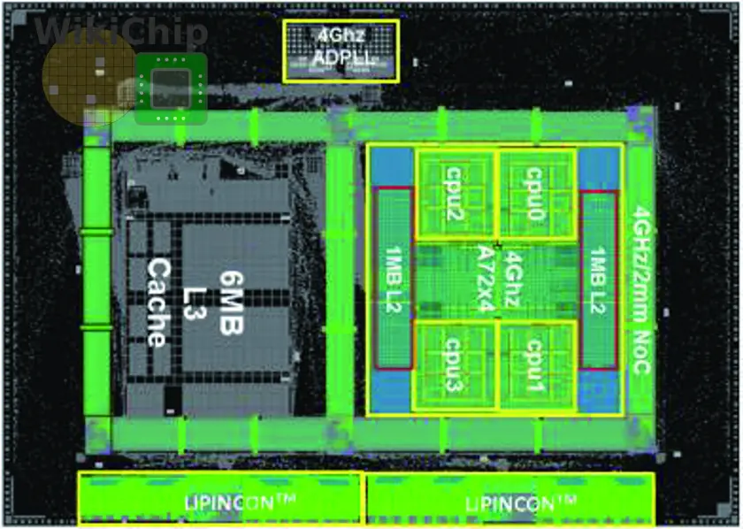
The chip itself is a dual-chiplet design, but the technology itself can scale to a larger number of chiplets with the additional PHYs with relative ease. Each chiplet is manufactured on TSMC 7-nanometer node with 15 metal layers. The die itself is just 4.4 mm by 6.2 mm (27.28 mm²). TSMC incorporated four Arm Cortex-A72 cores. Those are implemented using the high-performance cells (7.5T, 3p+3n) along with a custom-designed level 1 cache macros optimized for turbo frequencies >4GHz voltage operations. There are two L2 cache blocks. Each is 1 MiB. Those are implemented using their high-current bitcells and operate at half speed. Additionally, there is a large 6 MiB L3 cache that’s implemented using the high-density bitcells and operate at quarter-speed.
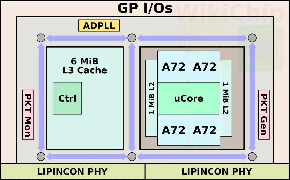
TSMC applied most of the usual enhancements you find in high perf chip. A typical h-tree was used to reduce clock distribution skew from 22ps to 8ps. Productive clock skew as well as via towers were used extensively to further improve timing on critical paths. In total, there are five voltage domains – 0.8V SoC, 0.8V ADPLL, 0.3-0.8V LIPINCON, 0.8V L3, and 0.3-1.2V for the CPUs. The chip features an all-digital PLL with a less than 10ps jitter which is used to generate the three clock domains for the CPUs, interconnect, and memory.
At a voltage of 1.20, the Cortex cores can reach 4 GHz (signoff). Numbers are based on the cores running Dhrystone pattern workload.
| Cortex-A72 | |||||
|---|---|---|---|---|---|
| Frequency | 2.8 GHz | 3.0 GHz | 3.5 GHz | 4.0 GHz | 4.2 GHz |
| Voltage | 0.775 V | 0.825 V | 0.95 V | 1.20 V | 1.375 V |
Mesh Interconnect
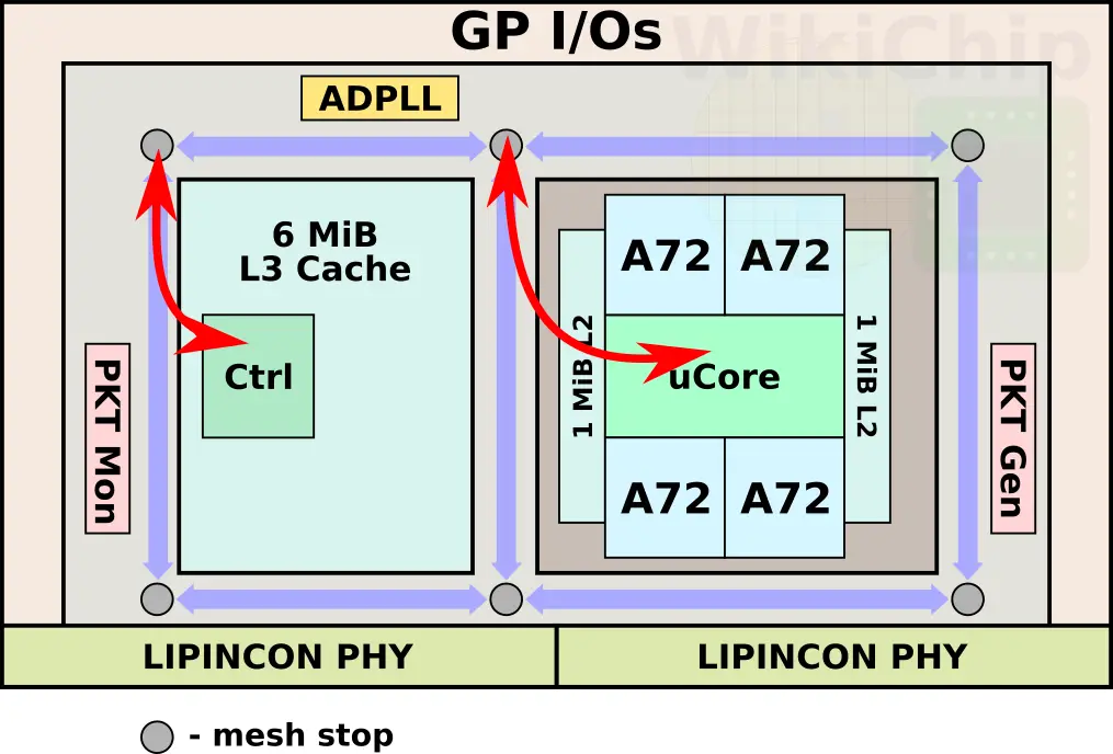
The die includes a mesh interconnect. Testing of the interconnect can be done via the on-die packet generation unit and packet monitoring unit. There are six bi-directional flip-flop mesh stations – one on each edge and two more in the middle. Those stations are surrounding the entire chiplet spaced roughly 2 mm apart. The mesh interconnect is 1968-bit wide and are routed in M12 and M13 using bit-wise-interleaved wires with opposite direction signals to minimize coupling. All in all, the on-die mesh interconnect can operate well above 4 GHz (0.8 V) up to 5 GHz (1.2 V). Both the cache and the Cortex cluster are connected to the nearest bottom-left mesh stop (when oriented vertically).
The interconnects can reach a frequency of 4 GHz at 0.76 V.
| Mesh Interconnect | |||||||
|---|---|---|---|---|---|---|---|
| Frequency | 2.0 GHz | 3.0 GHz | 3.5 GHz | 4.0 GHz | 4.5 GHz | 5.0 GHz | 5.2 GHz |
| Voltage | 0.52 V | 0.60 V | 0.68 V | 0.76 V | 0.90 V | 1.05 V | 1.18 V |
Inter-chip link
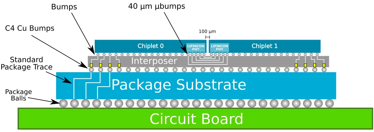
There are two Low-voltage-In-Package-INterCONnect (LIPINCON) interfaces on each chiplet. Each PHY measures just 0.42 mm by 2.4 mm (1.008 mm²). Those are single-ended, unidirectional, low-swing interfaces. One interface serves as a master for the CPU communication to the L3 while the second is a slave for the opposite direction. Unlike the rest of the SoC, due to power-ground noise concerns, there is a standalone PLL for a dedicated clock. Each PHY uses a 2:1 multiplex function in order to double the speed to 8 Gb/s. There are two DLLs for each sub-channel: one reduces the PVT variations while a second one is used to reduce clock skew, aligning the clock phase between SoC and PHY. Since a single-phase PLL is used, two loops are employed – the first locks the incoming clock period and divide it into eight phases while the second loop sub-divides that phase into 16 steps. In other words, at 4 GHz (250 ps), you are looking at sub 2 ps resolution.
For this paper, two dies were linked together. The second chiplet is rotated 180 degrees for the LIPINCON PHY abutment.
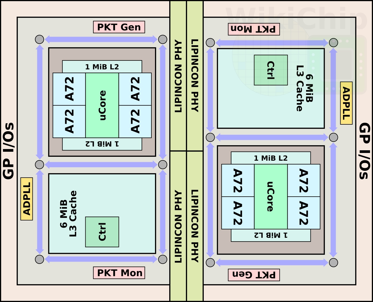
The chip itself uses TSMC CoWoS (chip on wafer on substrate) 2.5D packaging technology. This means a silicon interposer serves as a substrate for the two identical chiplets which are mounted on top of it. The use of a silicon interposer provides the ability to use much smaller bumps, enabling denser and lower power wires between the chiplets. In this design, a very aggressive micro-bump pitch of 40 µm are used and the two dies are separated by only 100 µm.

|
|
Technology Comparison
At twice the clock speed, the PHYs operate at a rate of 8 GT/s. With an interconnect width of 320-bit, the total bandwidth between the two dies is 320 GB/s. At a bump pitch of 40 µm, this is actually one of the more aggressive pitches we have seen among the recent chiplet designs. It also works out to a data flux of 1.6 Tb/s/mm². The comparison table below shows this chip against the two recent chiplet designs by AMD and Intel. It’s worth pointing out that Intel has previously talked about EMIB with bump pitches of 45 µm and even double the current density to 35 µm. However, so far, we are not aware of any Intel product that demonstrates those capabilities (Including Kaby Lake G).
| Recent Chiplet-based Designs | |||
|---|---|---|---|
| Company | Intel | AMD | TSMC |
| Chip | Stratix 10 | Zen | This |
| Packaging Technology | EMIB | MCM | CoWoS |
| Channel | 1 mm | N/A | 500 µm |
| Chiplet I/O Bumps | 55 µm | 150 µm | 40 µm |
| Interconnect | AIB | IF | LIPINCON |
| Data Rate | 2 GT/s | 10.6 GT/s | 8 GT/s |
| Power | 1.2 pJ/bit | 2 pJ/bit | 0.56 pJ/bit |
–
Spotted an error? Help us fix it! Simply select the problematic text and press Ctrl+Enter to notify us.
–