
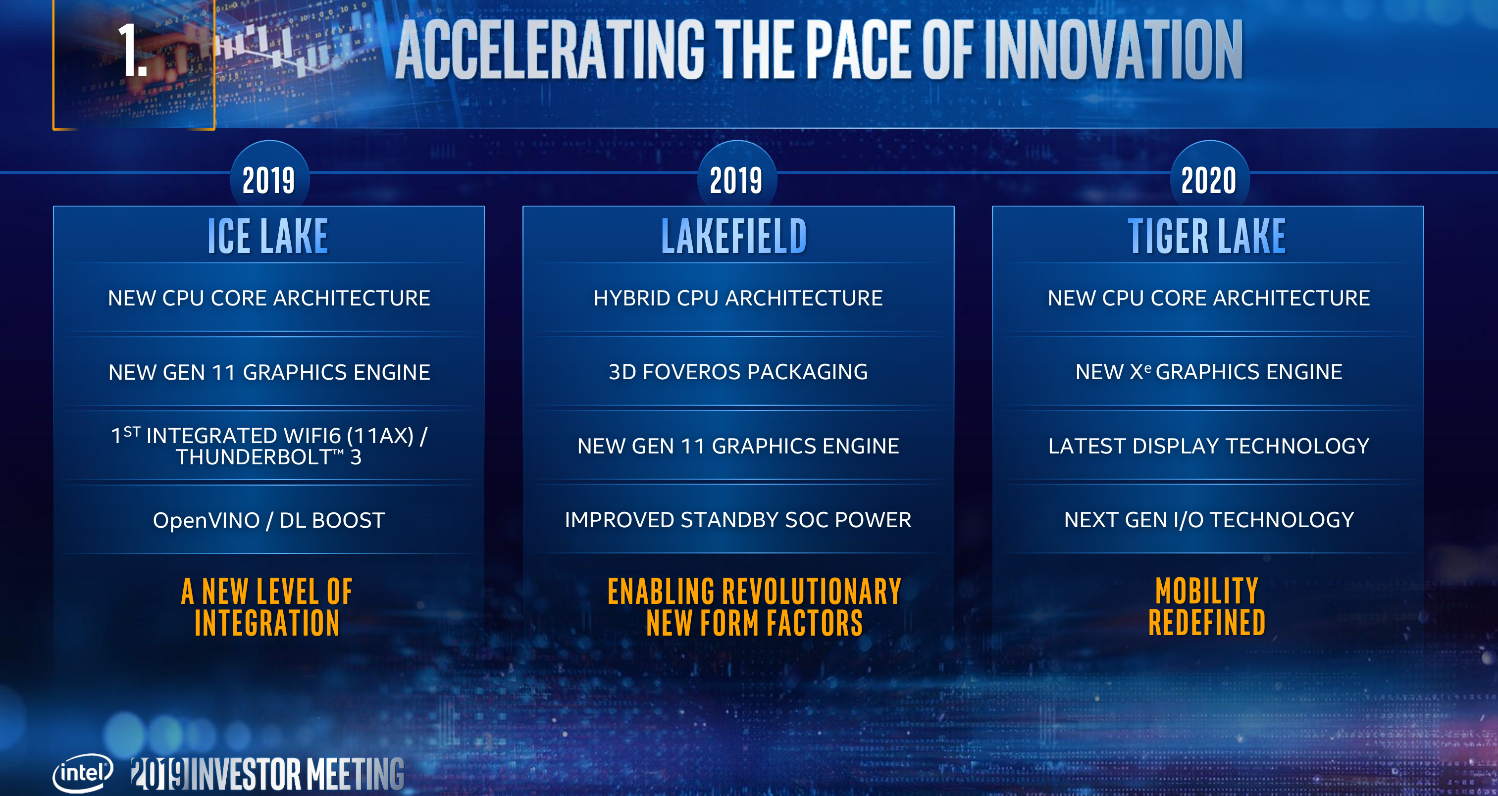
Ice Lake Brings A New CPU, GPU, IPU, and I/Os, To Follow By Tiger Lake Next Year
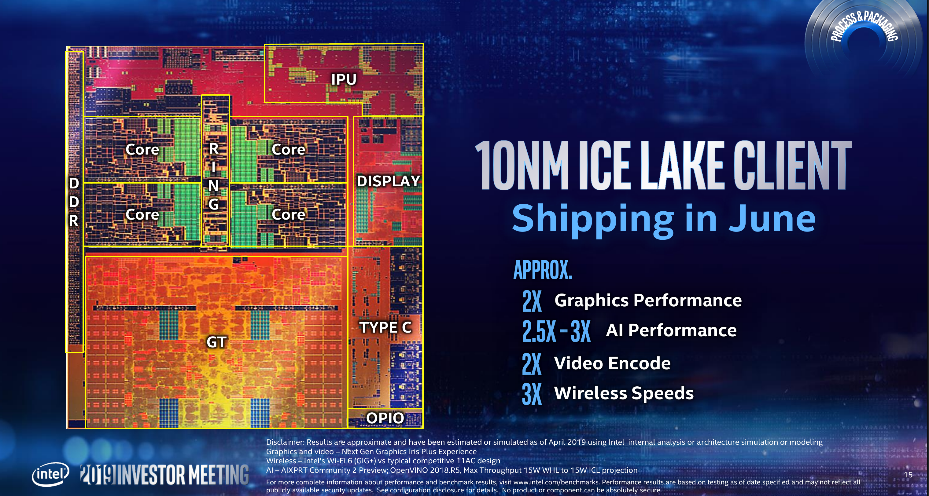
Intel’s long-awaited 10nm process has finally ramped earlier this year. The company’s first high-volume product is the mobile SoC codename Ice Lake which starts shipping in less than four weeks. Manufactured on 10nm+ process, the new chip will feature new CPU, GPU, and IPU architectures.
This article is part of a series that details Intel’s Investor Meeting.
1. Intel Process Technology And Packaging Plans: 10nm in June, 7nm in 2021
2. Ice Lake Brings A New CPU, GPU, IPU, and I/Os, To Follow By Tiger Lake Next Year
See also our series that details Intel’s Architecture Day.
1. Advanced 3D Packaging For More-than-Moore to Supplement 10- and 7-Nanometer Nodes
2. Intel Discloses 10nm Sunny Cove and Core Roadmap, Teases Ice Lake Chips
Ice Lake U
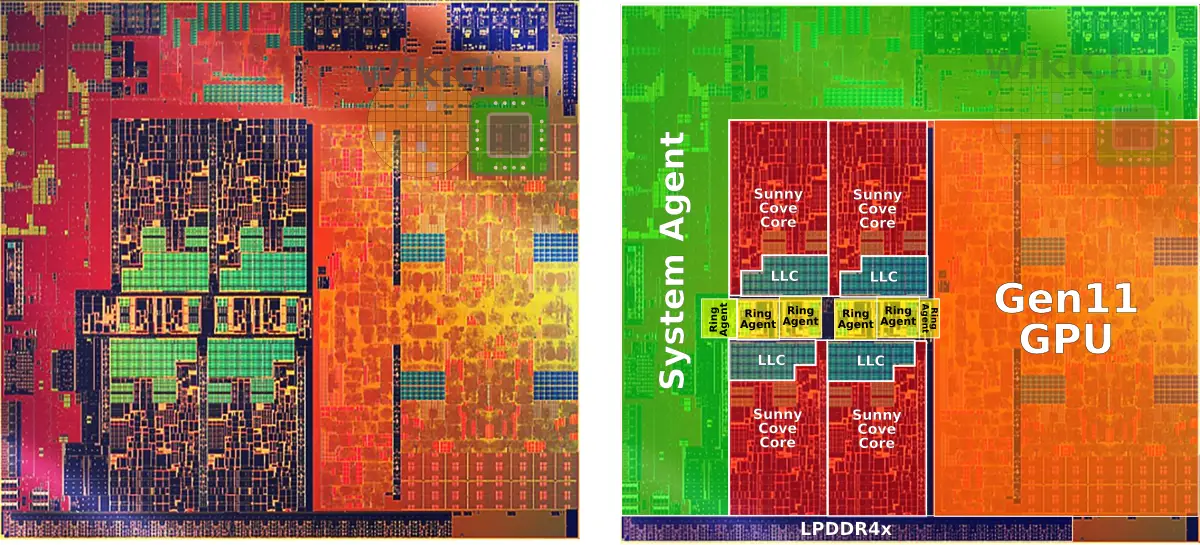
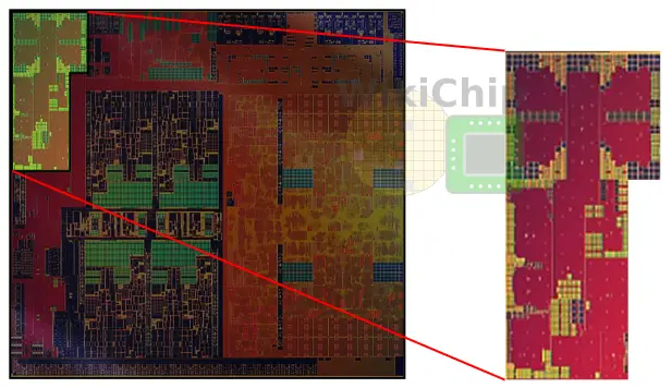
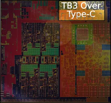
Ice Lake U processors are shipping in June. Similarly to currently shipping Whiskey Lake U parts, those chips will have up to four cores. Intel published a die shot of Ice Lake which reveals some new information about the chip itself. Ice Lake continues to use a ring interconnect with a ring agent per core and two additional ring agents at the system agent and GPU. It also appears that there is now a fully-integrated voltage regulator (FIVR) next to each core, one for the system agent, and two for the GPU.
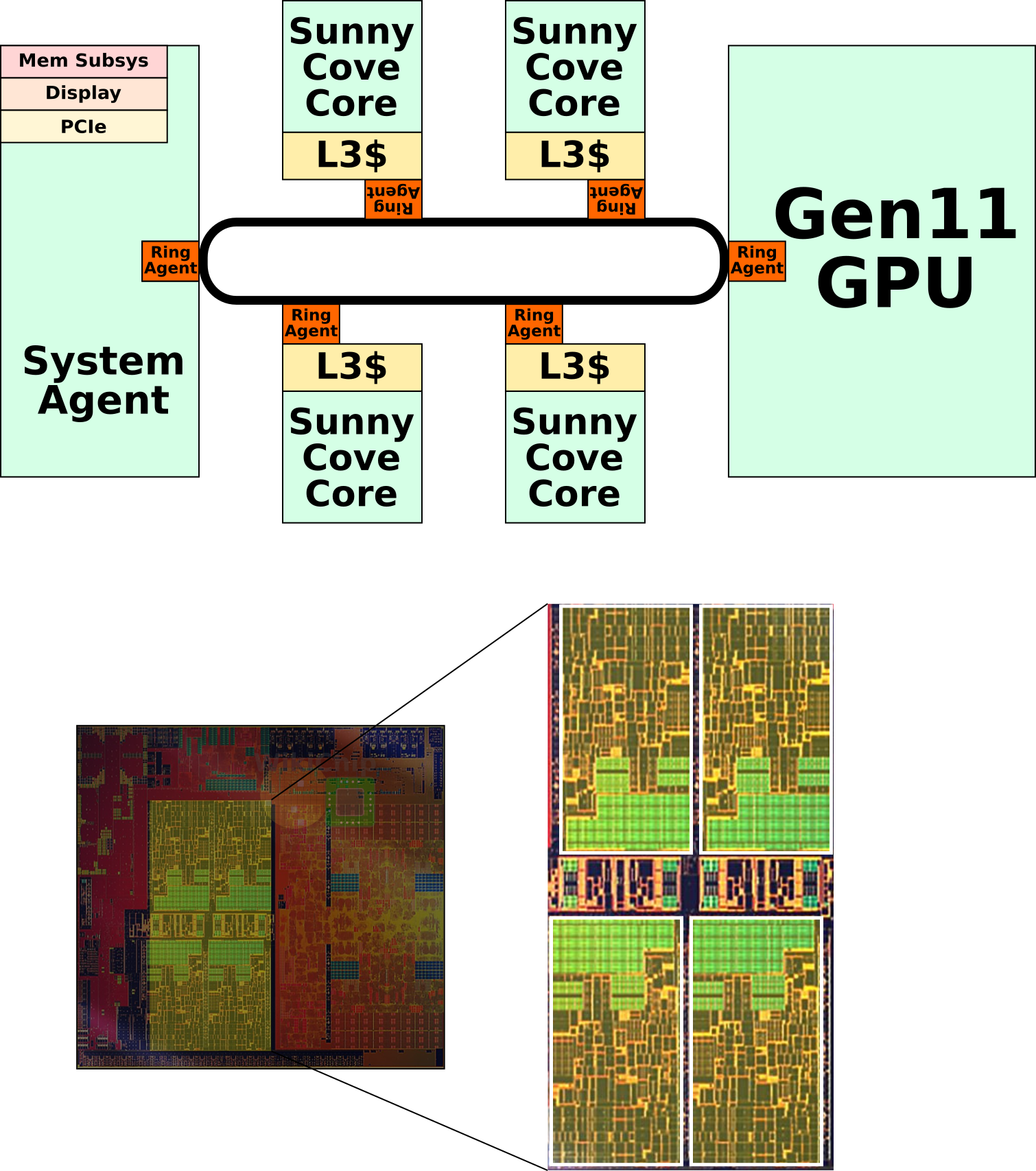
Sunny Cove core
One of the major changes in Ice Lake is the new Sunny Cove core – a core that Intel says will bring a significant improvement in IPC. This is the first new core since Skylake which was introduced nearly half a decade ago. Sunny Cove increases the cache sizes for the first time in over two decades. One of those changes is the L1 data cache size which has increased in capacity by 50% to 48 KiB. Likewise, the L2 cache has been doubled to 512 KiB. The scheduler on Sunny Cove has been further widened – 25% wider than Skylake, enabling up to 10 operations may be dispatched each cycle.

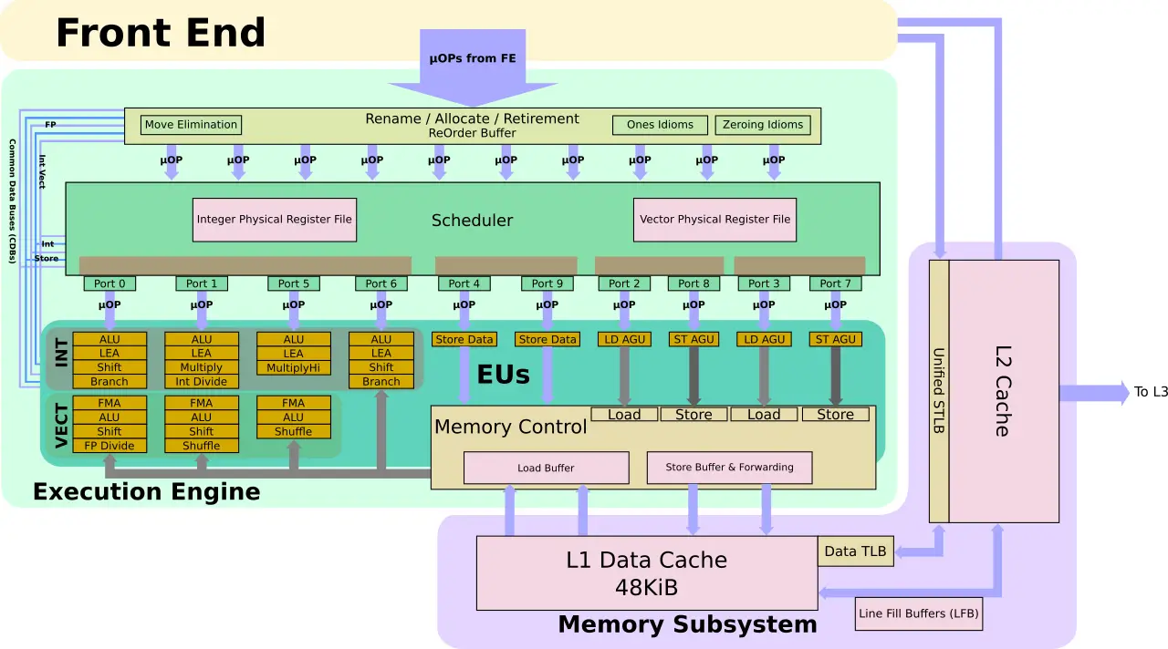
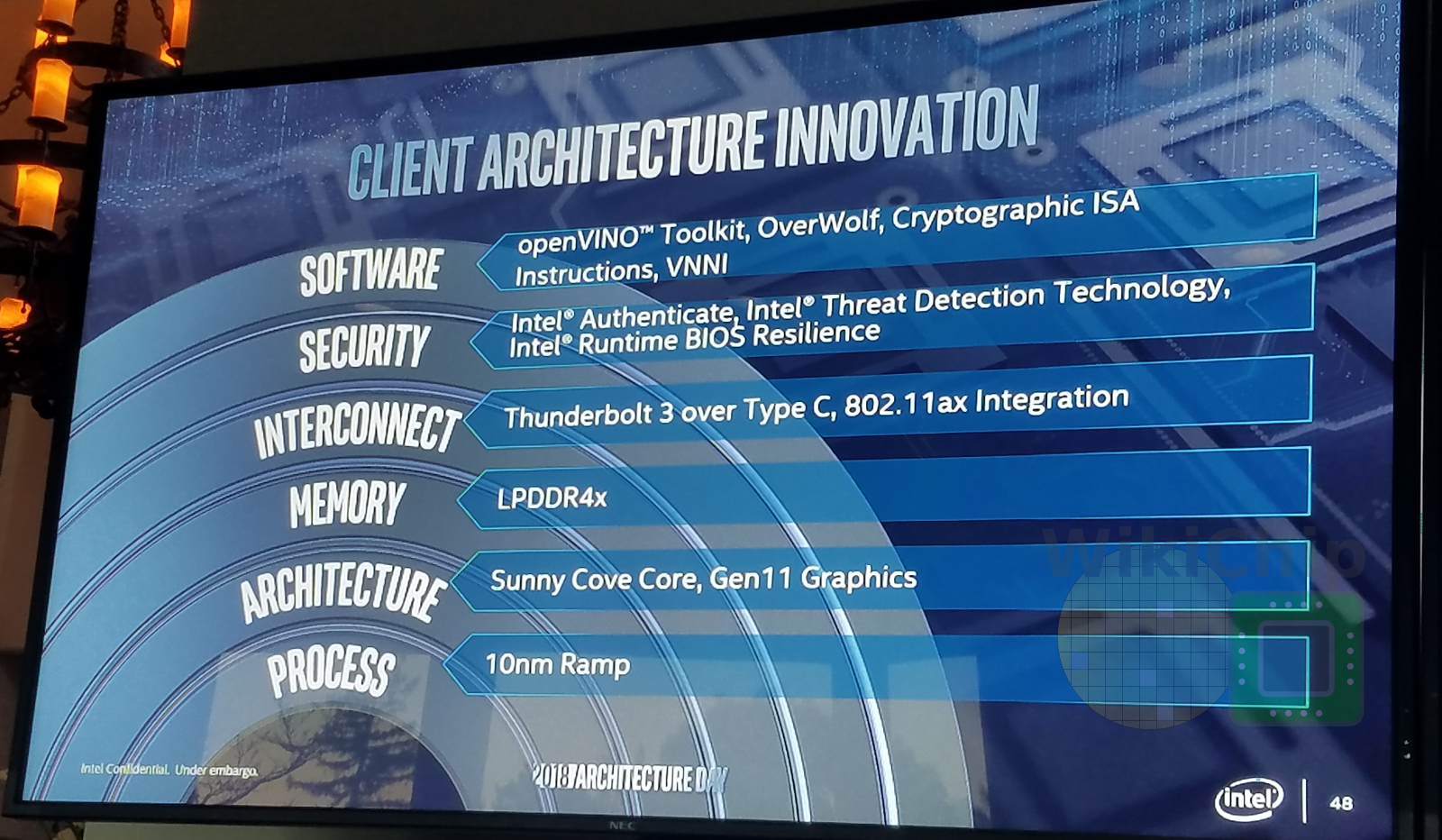
Beyond being wider and more complex, this is also the first Intel client core to introduce AVX-512. Compared to Skylake, Sunny Cove has a number of new very welcomed AVX-512 extensions which brings type orthogonality to the instruction set as well as extensions for deep learning and cryptography acceleration. It also incorporates the VNNI extension which has been designed to accelerate inference processing. One of the applications that makes use of that extension is Windows which allows the user to search their photos using AI. AI is used to identify objects and scenes that appear in the photos and makes them searchable. Beyond this, Intel offers the OpenVINO toolkit which allows developers to make use of those hardware capabilities in their software.
Gen11 Graphics
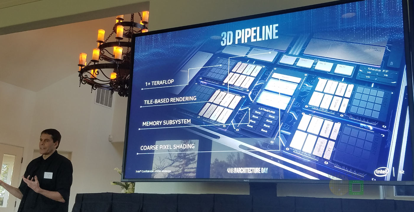
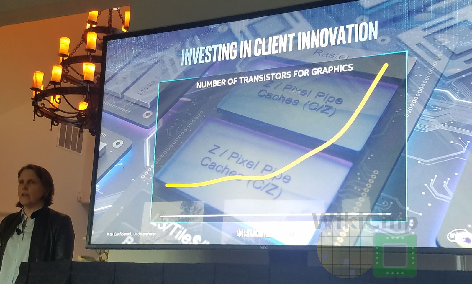
With a larger GPU, there is a need for higher memory bandwidth. For this reason, Ice Lake U moved to LPDDR4x with four 32-bit channels. Though no official specifications have been revealed, Intel expected memory bandwidths in the range of 50-60 GB/s which puts the memory controller at around 3733 MT/s with a 128-bit bus. This is roughly twice the bandwidth of current Whiskey Lake chips. The GPU on Ice Lake is based on their Gen 11 architecture which is drastically different from Gen9.5. The new GPU introduces tile-based rendering (TBR) as well as coarse pixel shading (CPS). The slice common has been greatly enhanced. It now houses a 3-times larger L3 that’s better partitioned and is split between eight banks. The execution units have also been reworked. There is now almost thrice as many EUs albeit certain operations have reduced throughput. Intel dropped double-precision in favor of light-weight emulation. All in all, with up to 64 execution units, the new GPU supports up to 1,024 single-precision floating point operations per cycle. At 1 GHz, this GPU can now deliver up to a teraFLOP of performance. The impressive feat was achieved while reducing the area by 25% iso-process compared to Gen9.
4th Gen IPU
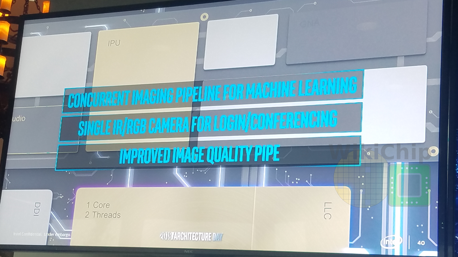
Ice Lake integrates Intel’s 4th generation Image Processing Unit (IPU). The IPU was first added with the dual-core Skylake mobile processors back in 2015. The 4th Gen IPU found in Ice Lake introduces a number of new enhancements. There is now support for 4K 30fps video capture support. Additionally, new hardware support for better de-noising has been implemented which can support 16 MP stills in low light conditions. The new IPU also has a concurrent image pipeline, supporting multiple different processing from the same camera streams, allowing a single camera to take the functionality of multiple sensors. A common example of that is devices with both IR and RGB cameras in the laptop bezel which can now be changed to a single camera. Intel says they are exposing more registers from the IPU to software in order to provide more flexibility for applications that make use of that for machine learning. It’s also worth noting that Intel integrated the MIPI interface onto the processor as well. Previously that was found on the chipset. The change significantly improves the latency, a required attribute needed for more advanced ML-specific applications. Some of those changes are designed to form the foundation for future generations of improvements.
I/O
In addition to the new LPDDR4x controller, Ice Lake U also introduces Thunderbolt 3 over Type C natively on-die. Previously this required a large set of chips on the motherboard to support the full functionality. In Ice Lake, all of that has been moved off the board and has been integrated on-die. The one exception being the high-voltage power delivery subsystem which has been left off-die.
Tiger Lake
Also planned for 10nm+, Tiger Lake will succeed Ice Lake next year. Intel says every component on Tiger Lake has been rearchitected. This includes a new core – presumably based on Willow Cove, new integrated graphics based on Intel’s Xe architecture, a new display engine, and next-generation of I/O. Intel says the Tiger Lake silicon is back from the fab and has booted Linux and Windows.
Graphics
Tiger Lake quad-core solution with a 15W TDP will feature Xe (GT2) integrated graphics with up to 96 execution units. 50% more EUs than Ice Lake U Gen11 graphics and 4 times more than currently shipping Whiskey Lake U Gen9.5 graphics. It’s worth noting that since Tiger Lake is back from the fab, Intel’s discrete client graphics solution, codename Arctic Sound, should be in a similar situation. Gregory Bryant noted that they are still on track for a 2020 launch for their discrete client graphics solution.
| Intel Integrated GPUs | ||||||
|---|---|---|---|---|---|---|
| SoC | Ivy Bridge | Haswell | Broadwell | Skylake | Ice Lake | Tiger Lake |
| GPU | Gen7 | Gen7.5 | Gen8 | Gen9 | Gen11 | Xe |
| EUs (GT2) | 16 | 20 | 24 | 24 | 64 | 96 |
| L3$ | 512 KiB | 512 KiB | 768 KiB | 768 KiB | 3 MiB | ? |
| Half-Precision (FLOPs/cycle) |
– | – | 768 | 768 | 2,048 | ? |
| Single-Precision (FLOPs/cycle) |
256 | 320 | 384 | 384 | 1,024 | ? |
| Double-Precision (FLOPs/cycle) |
64 | 80 | 96 | 96 | – | – |
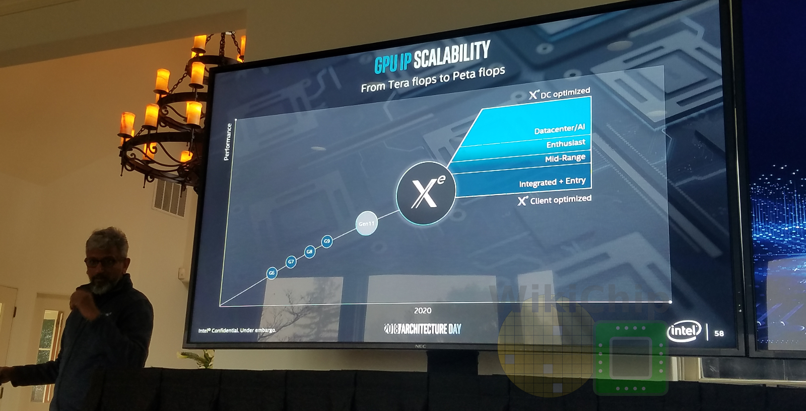
It’s worth pointing out that Raja noted that Xe GPUs are intended to scale all the way from integrated and entry-level up to data center and HPC applications.
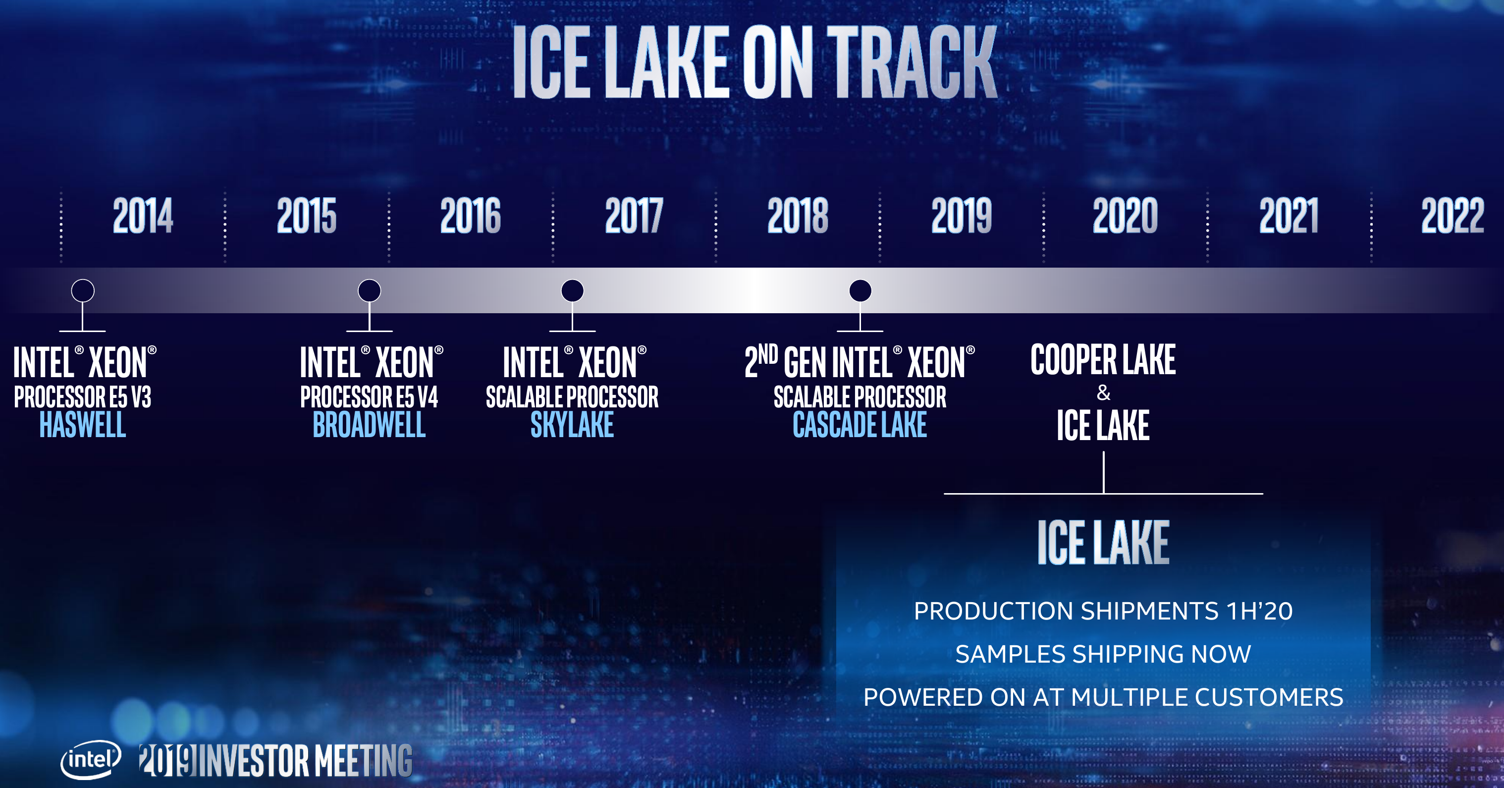
Ice Lake Server
Server CPUs based on the Ice Lake server microarchitecture will fast-follow their client chips in the first half of 2020. Ice Lake servers and Cooper Lake servers will both be on the same platform codename Whitley. Cooper Lake is said to offer higher core count over Cascade Lake with Ice Lake providing higher single-thread performance. Ice Lake server CPUs are already sampling and will start production in the first half of 2020.
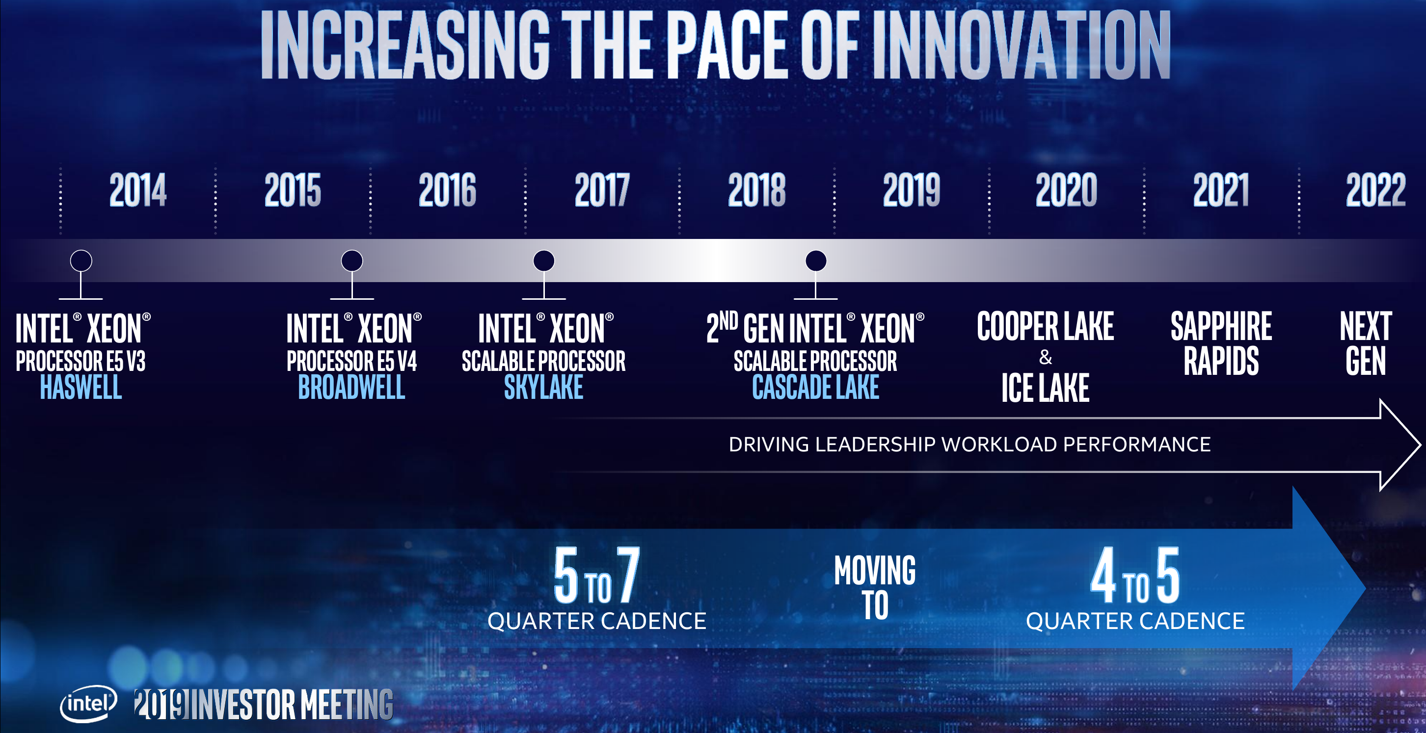
Shorter Cadence
One of the topics touched on during Navin Shenoy’s presentation was the cadence of their server CPU releases. While historically, Intel rolled out a new CPU architecture every five to seven quarters, Navin stated that Intel will be shifting to a much shorter iteration rate. Intel plans on release a new server CPU architecture on roughly a yearly cadence. Cooper Lake and Ice Lake servers will launch in early 2020 and those will follow after roughly a year with Sapphire Rapids launching in 2021. Cooper is made on Intel’s 14-nanometer process, Ice Lake is on 10nm+, and Sapphire Rapids will make use of 10nm++ technology.
7NM Xe GPGPUs
In a surprising move, Intel announced that their first and lead 7-nanometer product will be their general-purpose Xe GPU targeting data center and HPC applications. “It’s a major strategic priority for Intel,” Renduchintala said. This product is a chiplet-based design and will make use of Intel’s next-generation Foveros 3D technology. This product will launch in 2021 and will be used in the US first exascale supercomputer, Aurora for the Department of Energy. Given the time constraints on this, we should expect to see serious movement on their 7-nanometer side late next year.

–
Spotted an error? Help us fix it! Simply select the problematic text and press Ctrl+Enter to notify us.
–